Improving the Astable Mulitvibrator Circuit
In a previous article, we built and described the operation of a classic astable mulitvibrator that used two NPN transistors and a few supporting components. It was a good basis for a multi-use oscillator, but had a major limitation in its ability as a practical circuit. By its nature, the output waveform had a rounded leading edge, which was unsuitable for many applications. In this article, we will improve that circuit so that it generates a clean square wave, by adding only four components.
Before building a breadboard, please review our safety procedures and recommendations page.
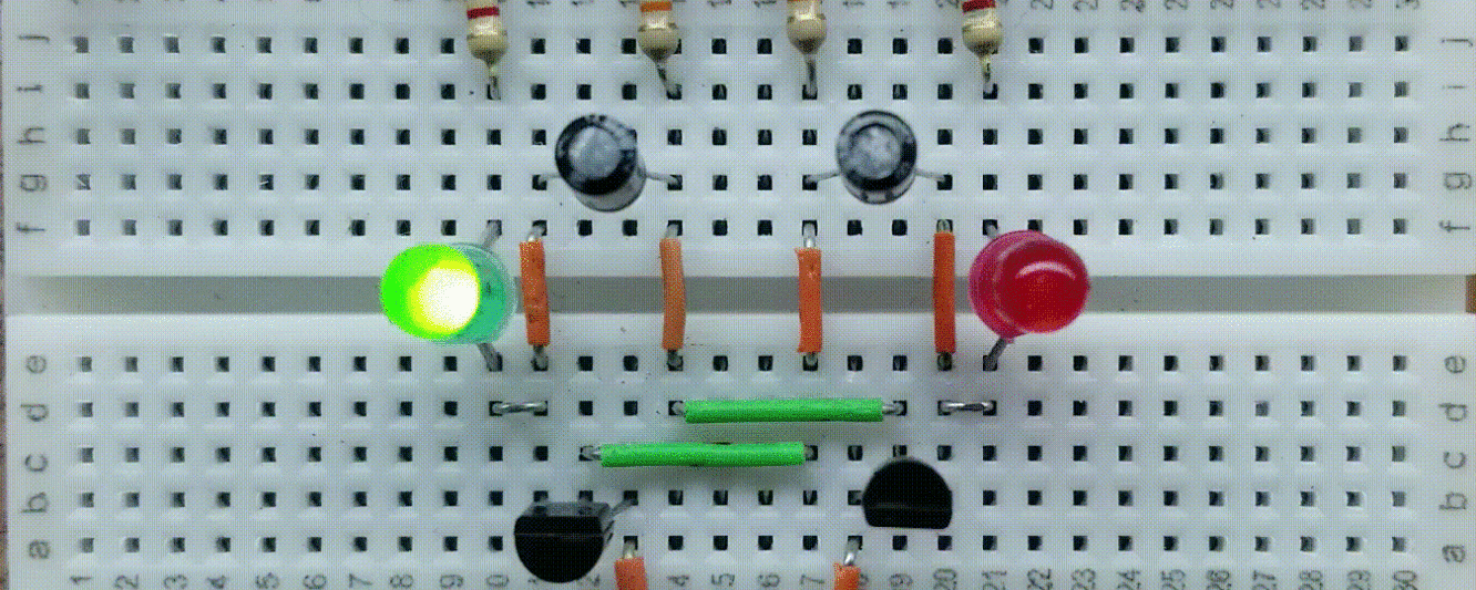
A picture of the breadboarded improved mulitvibrator circuit is shown below.
Supplies Needed
Supplies needed for this project:
- Minimum breadboard equipment (see here)
- (2) 6.8k ohm 1/4 watt resistors
- (3) 1k ohm 1/4 watt resistors
- (2) 27k ohm 1/4 watt resistors
- (2) 0.1uF 16v Mylar capacitors
- (4) 2n3904 transistors
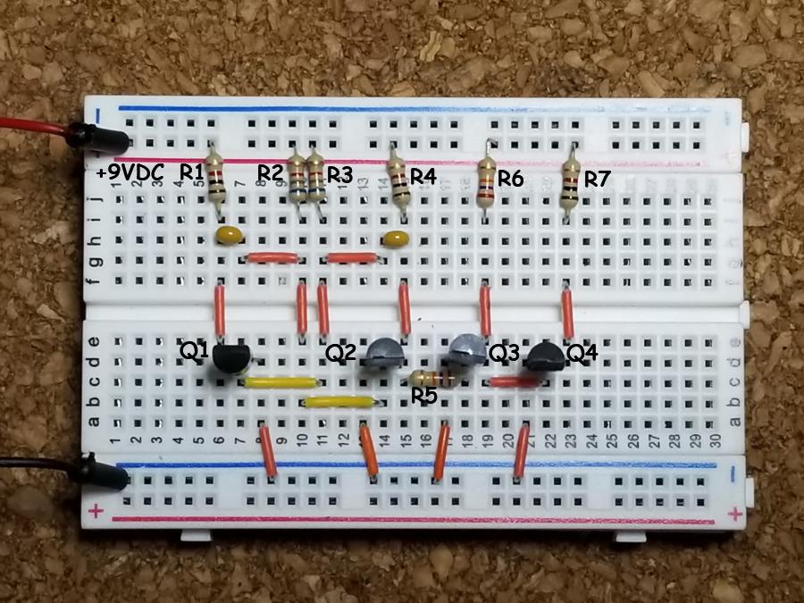
Construct the circuit exactly as shown on the breadboard, observing the orientation of the 2n3904 NPN transistors. Notice that Q1 is facing backward. Q2 and Q3 is facing forward. If you already constructed the mulitvibrator in the basic astable mulitvibrator project, you can easily modify it for this project. Scroll down to the bottom of this article to see the full schematic.
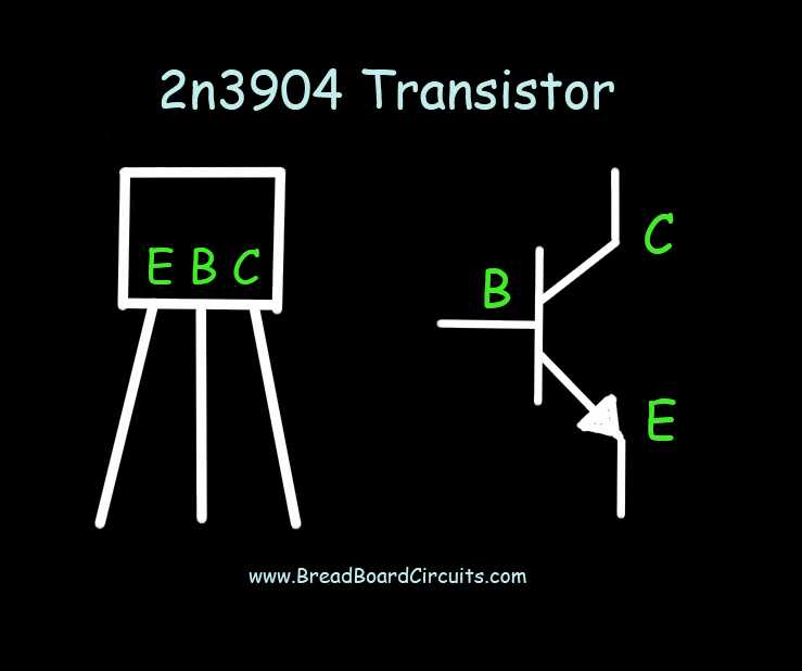
The 2n3904 NPN Transistor
Below is both the pinout (with the transistor facing forward) and symbol for the 2n3094 transistor. “E” stands for Emitter, “B” stands for Base, and “C” stands for Collector.
Frequency Selection
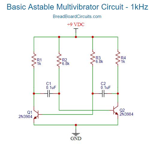
This article won’t describe the basic mulitvibrator operation. That is described in detail in the basic astable mulitvibrator project. The mulitvibrator we’ll construct for this project will be calculated to have an approximate oscillation frequency of 1KHz. The reason we choose this frequency is that it is a common minimum frequency used for LED dimming and this circuit will serve as the basis for a separate pulse width modulation project. Also, a 1KHz output frequency will better show the leading edge rounding associated with the basic astable mulitvibrator circuit. The timing components are R2/C1 and R3/C2. Since we want a 50% duty cycle, R2=R3 and C1=C2. The formula as found in the classic astable multivibrator article is R=0.72/(fxC). By selecting a common 0.1uF value, we can find R. So R=0.72/(1KHz x 0.0000001) = 7200 Ohms. We selected the 6.8k Ohm resistor because it was more readily available.
Basic Multivibrator Schematic
Below is a schematic of the basic astable multivibrator circuit for this project, that we will add a few components to in order to yield a nice square wave.
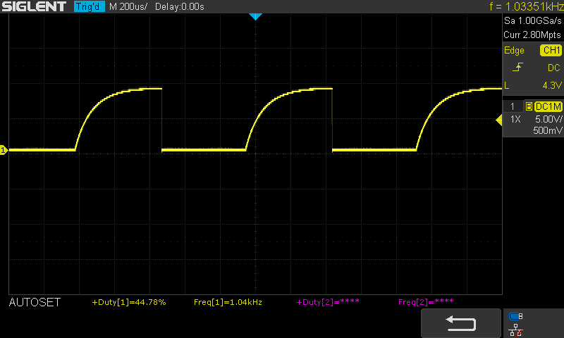
Basic Multivibrator Output Waveform
Mulitvibrator Clean-up Stage
Suppose you wanted to use this to drive a high-power LED flasher. The above waveform wouldn’t be suitable for that because you’d want a sharp rise time so that the device driver be either in its “off” or “on” state. A slow rise time at the device’s input will cause it to partially operate in its “active” region, which means that there will current flowing through the device AND a voltage drop across it at the same time. That leads to excess power dissipation of the device, and diversion of power from the high-power LED to the device itself.
So let’s take that rounded waveform output and turn it into a real “square wave”. We can do so with only a few extra components – in fact, only two more general purpose transistors and two resistors.
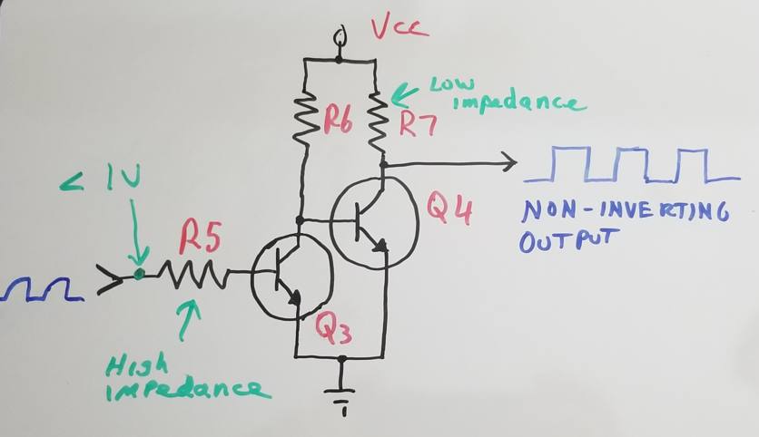
First we will take the raw mulitvibrator output and use it to drive a simple NPN low-side switch. This stage effectively cuts off whole leading edge of the raw input, because Q3 will saturate as soon as the base reaches 0.7 volts. A base resistor needs to be on that switch though to both isolate the basic mulitvibrator output from the cleanup stage and to limit the base current. There will have to be some voltage drop across that base resistor though – which means we can’t cut the raw waveform off right at 0.7 volts. To reduce that voltage drop, we can add another amplification stage using another transistor.
Given that configuration, we can come up with some design criteria:
Design Criteria
- Input stage trigger voltage less than 1 volt. (this cuts the rounded portion of the waveform off early on)
- High impedance input. (so that the clean-up stage has as little effect on the basic mulitvibrator as possible)
- Low impedance output. (so the cleaned-up output can drive other circuits)
- Non-inverting output.
Below shows the clean-up stage configuration based on the design criteria:
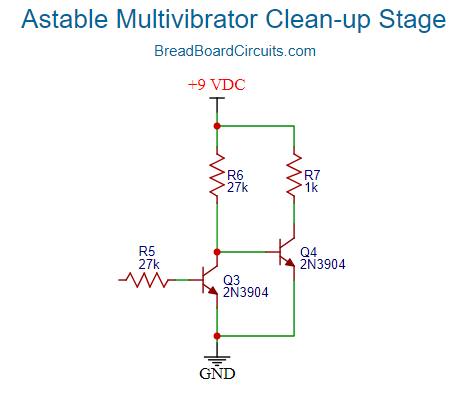
Selecting a value of 1k for R7 gives a low enough output impedance to drive most other circuits. Working backward using the beta of the 2n3904, the value 27k Ohms was selected for R5 and R6. Because the output stage has a gain of greater than 22,000, the current through R5 needed to fully saturate Q3 and switch the stage “on”, is only 10uA, which translates to a voltage of 0.75 volts on the left side of R5. So any part of the raw waveform’s leading edge above that gets cut off. That effectively removes the whole front-end of the rounded square wave and produces a clean square wave output. The output stage with the final selected component values is shown below.
Finalized Multivibrator Clean-up Stage
Below shows the clean-up stage schematic with the selected component values.
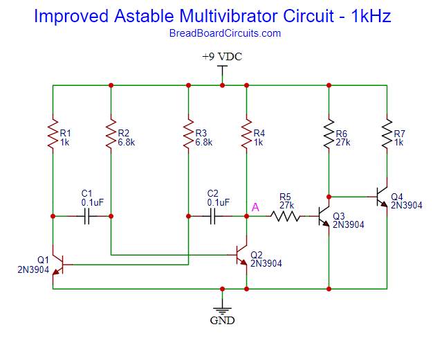
Full Schematic for the Improved Multivibrator
Adding the finalized clean-up stage to the classic astable multivibrator circuit yields the circuit below.
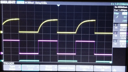
Improved Waveform Output Compared to Raw Input
Adding that stage cleaned up that raw waveform nicely. An image of the raw waveform (in yellow) compared to the inverted improved waveform (in purple) is shown below.
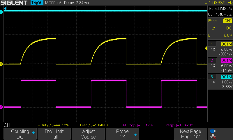
As the image shows, the lower waveform as compared to the top one is an actual square wave with the desired sharp transitions.. The improved wave shape is more suitable for driving high-current devices, digital circuits, and anything that requires a square wave input.
For a better experience building breadboarded circuits, please see our page detailing the minimum recommended lab equipment for your electronics bench. Also, don’t forget to review the recommended safety procedures to follow when building and testing breadboarded circuits.
Finally, for other interesting breadboarded circuits please visit the home page here or our YouTube channel here.
SM
We are a participant in the Amazon Services LLC Associates Program, an affiliate advertising program designed to provide a means for us to earn fees by linking to Amazon.com and affiliated sites.