CN100559326C - Low voltage detection system - Google Patents
Low voltage detection system Download PDFInfo
- Publication number
- CN100559326C CN100559326C CNB038250209A CN03825020A CN100559326C CN 100559326 C CN100559326 C CN 100559326C CN B038250209 A CNB038250209 A CN B038250209A CN 03825020 A CN03825020 A CN 03825020A CN 100559326 C CN100559326 C CN 100559326C
- Authority
- CN
- China
- Prior art keywords
- voltage level
- voltage
- power supply
- lead wire
- supply lead
- Prior art date
- Legal status (The legal status is an assumption and is not a legal conclusion. Google has not performed a legal analysis and makes no representation as to the accuracy of the status listed.)
- Expired - Fee Related
Links
Images


Classifications
-
- G—PHYSICS
- G06—COMPUTING; CALCULATING OR COUNTING
- G06F—ELECTRIC DIGITAL DATA PROCESSING
- G06F1/00—Details not covered by groups G06F3/00 - G06F13/00 and G06F21/00
- G06F1/26—Power supply means, e.g. regulation thereof
- G06F1/32—Means for saving power
- G06F1/3203—Power management, i.e. event-based initiation of a power-saving mode
-
- G—PHYSICS
- G06—COMPUTING; CALCULATING OR COUNTING
- G06F—ELECTRIC DIGITAL DATA PROCESSING
- G06F1/00—Details not covered by groups G06F3/00 - G06F13/00 and G06F21/00
- G06F1/26—Power supply means, e.g. regulation thereof
- G06F1/28—Supervision thereof, e.g. detecting power-supply failure by out of limits supervision
-
- G—PHYSICS
- G06—COMPUTING; CALCULATING OR COUNTING
- G06F—ELECTRIC DIGITAL DATA PROCESSING
- G06F1/00—Details not covered by groups G06F3/00 - G06F13/00 and G06F21/00
- G06F1/26—Power supply means, e.g. regulation thereof
- G06F1/30—Means for acting in the event of power-supply failure or interruption, e.g. power-supply fluctuations
Abstract
The low-voltage that is used for logical unit detects that (LVD) system is included in a LVD circuit (110) that indication is provided when power supply lead wire voltage (109) drops under first voltage level and the 2nd LVD circuit (116) of interruption (118) is provided under power supply lead wire voltage drops to second voltage level time.In one embodiment, therefore the 2nd LVD circuit starts selectively than a LVD circuitry consumes more power.In one embodiment, power supply lead wire voltage between first and second voltage levels and logical unit be in and stop or during low-power mode, the 2nd LVD circuit period property ground starts to detect power supply lead wire voltage.In the time of under power supply lead wire voltage is reduced to second voltage level, logical unit is placed in safe condition, and logical unit is under an embargo and admits to interrupt in this safe condition, rises on first voltage level up to power supply lead wire voltage.
Description
Technical field
The present invention relates to low voltage detection system in general, more specifically to low voltage detection system with a plurality of voltage detecting level.
Background technology
In many battery powered systems, such as the system of portable electronic industry, logical unit plays certain effect such as microprocessor and microcontroller in master controller and/or power management block.On this, importantly, faint or be removed the internal logic states and the volatile memory (RAM, control register, logic state etc.) of time protection logical unit at battery electric power.For example, in nowadays available microcontroller, low-voltage detects (LVD) electric circuit inspection and when produces low-voltage and microcontroller is resetted.Replacedly, some LVD system allows the interruption of microcontroller reception except resetting, so that microcontroller is placed stop mode with software so that the current drain minimum is recovered up to cell voltage.Yet, in these systems,, still may receive interruption (such as from keyboard input) though be in the stop mode, cause microcontroller before battery recovery, to be started once more and make battery consumption, cause loss of data thus.
Summary of the invention
Therefore, need provide a kind of LVD system, the internal logic states of this system protection logical unit and volatile memory allow security recovery from electric power battery status faint or that be removed simultaneously.In addition, in order to reduce cost, need provide the system of the logical unit of the lead-in wire that a kind of use has minimum number.
According to first aspect present invention, a kind of integrated circuit (100) is provided, comprising: from the power supply lead wire (109) of power supply received power; First voltage detecting circuit (110) has output, and first voltage detection signal is provided, and when the voltage level that is used to refer to power supply lead wire is lower than first voltage level; Second voltage detecting circuit (116) has output, and second voltage detection signal is provided, and when the voltage level that is used to refer to power supply lead wire is lower than second voltage level, and this second voltage level is lower than first voltage level; CPU (central processing unit) (160), this CPU (central processing unit) are configured to from the power power supply that receives by power supply lead wire; Operatively be coupled to the interrupt handler (142) of CPU (central processing unit), this interrupt handler response comprises one group of interruption of at least one interruption; Interrupt handler control circuit (138), be used to control interrupt handler to comprising one group of response of interrupting of at least one interruption, this interrupt handler control circuit responds first voltage detection signal and responds first signal with first signal condition, this first signal condition indicates the voltage level of power supply lead wire indicated as second voltage detection signal at least, be reduced under second voltage level, wherein when first signal was in first signal condition, response comprised described one group of interruption of at least one interruption when interrupt handler control circuit startup interrupt handler was higher than first voltage level with the voltage level at first voltage detection signal indication power supply lead wire.
According to second aspect present invention, a kind of system that can carry out the battery power-on servicing is provided, comprise according to the described integrated circuit of first aspect present invention, and further comprise: be coupled to power supply lead wire to give the battery of power supply lead wire transmission power; With the external unit that operatively is coupled to integrated circuit by at least one signal wire pin of integrated circuit.
According to third aspect present invention, a kind of integrated circuit is provided, comprising: from the power supply lead wire (109) of power supply received power; First voltage detecting circuit (110) has output, and first voltage detection signal is provided, and when the voltage level that is used to refer to power supply lead wire is lower than first voltage level; Second voltage detecting circuit (116) has output, and second voltage detection signal is provided, and when the voltage level that is used to refer to power supply lead wire is lower than second voltage level, and this second voltage level is lower than first voltage level; Wake-up circuit (124), the output of this wake-up circuit (126) starts second voltage detecting circuit so that second voltage detection signal to be provided when the voltage level of first voltage detection signal indication power supply lead wire is lower than first voltage level.
According to fourth aspect present invention, a kind of integrated circuit is provided, comprising: from the power supply lead wire (109) of power supply received power; CPU (central processing unit) (160), this CPU (central processing unit) are configured to from the power power supply that receives by power supply lead wire; Voltage detecting system, this voltage detecting system is configured to provide the voltage level of power supply lead wire to be reduced to the indication of first under first voltage level (118), and be configured to provide the voltage level of power supply lead wire to rise to the indication of second on second voltage level (112), wherein first voltage level is lower than second voltage level; Operatively be coupled to the interrupt handler (142) of CPU (central processing unit), this interrupt handler response comprises one group of interruption of at least one interruption; The interrupt handler control circuit, be used to control interrupt handler to comprising one group of response of interrupting of at least one interruption, wherein when first signal (136) is in first signal condition, the voltage level of this first signal condition indication power supply lead wire is indicated as first indication, be reduced under first voltage level, this interrupt handler control circuit response second indication starts interrupt handler comprises at least one interruption with response described one group of interruption.
By technique scheme of the present invention, can overcome the defective of prior art.By with reference to following the drawings and specific embodiments, will make those skilled in the art further understand the features and advantages of the present invention.
Description of drawings
With non-limitative drawings explanation the present invention, identical in the accompanying drawings reference number is represented similar elements, wherein by way of example;
Accompanying drawing 2 is depicted as the accompanying drawing of the method that enters and withdraw from safe condition according to an embodiment of the present;
Accompanying drawing 3-5 is depicted as the truth table corresponding to the various unit in the data handling system in accompanying drawing 1;
Accompanying drawing 6 is depicted as the synoptic diagram of a kind of embodiment of the low-voltage detecting unit in the data handling system of accompanying drawing 1;
Accompanying drawing 7 is depicted as the synoptic diagram of a kind of embodiment of another low-voltage detecting unit in the data handling system of accompanying drawing 1;
What those of ordinary skills will appreciate that is not draw in proportion for the present invention's element in the accompanying drawings is described clear and concisely.For example, some size of component in the accompanying drawings can be amplified to help to understand embodiments of the invention with respect to other element.
Embodiment
Just as used herein, term " bus " is used to refer to can be used for transmitting a plurality of signals or the conductor of the information of one or more types such as data, address, control or state.Illustrate or description with reference to single conductor, a plurality of conductor, unidirectional conductor or bidirectional conductors at this conductor of discussing.Yet different embodiment can change the enforcement of conductor.For example, can use the unidirectional conductor of separation and do not use bidirectional conductors, vice versa.In addition, a plurality of conductors can substitute with the single conductor that the mode of serial or time-division is transmitted a plurality of signals.Similarly, the single conductor that transmits a plurality of signals can be broken down into the various conductor that transmits these signal subspace groups.Therefore, for the transmission of signal, there are many selections.
Use term " to claim " and " negating " (or falling tone claims) respectively when making signal, mode bit or similar devices be translated into logical truth or logical falsehood mentioning.If the logical truth state is a logic level 1, then the logical falsehood state is a logic level 0.If the logical truth state is a logic level zero, then the logical falsehood state is a logic level 1.
MCU 102 also comprises the LVD1 unit 110 that is coupled to the battery node 109 (being power supply lead wire) that voltage Vbatt is provided.When LVD1 110 detected under when Vbatt drops to the first voltage level LV1, MCU 102 comprised also when detection Vbatt drops to the LVD2 unit 116 under the second voltage LV2, and, usually LV1 is greater than LV2 here.MCU 102 also can comprise and is coupled to battery node 109 and LVD2 116 Vreg is offered the voltage regulator 114 of LVD2116.Yet in variant embodiment, voltage regulator 114 can not exist, and LVD2 116 is coupled to battery node 109 in this case.MCU 102 also comprises periodic wakeup unit (PWU) 124, PWU start unit 120, LVD2 start unit 128 and interrupt handler (IH) control module 138.Bus 152 offers LVD2 start unit 128 and PWU start unit 120 with STOP pattern indication STOP 132.LVD1110 offers PWU start unit 120 and IH control module 138 with signal LV1_Detect 112.PWU start unit 120 offers PWU 124 with signal PWU_en 122, and PWU 124 offers LVD2 start unit 128 with signal Wakeup 126.LVD2 start unit 128 offers LVD2 116 and voltage regulator 114 (if present) with signal LVD2_en 130.Safe bit register 134 offers PWU start unit 120 and IH control module 138 with signal safe 136.Interrupt handler 142 receives internal interrupt and passes through bidirectional conductors 148 from LVD2 116 received signal safe136, from IH control module 138 received signal IH_block 140, by bus 152 and receives external interrupt 144.
The external circuit of data handling system 100 comprises the battery 106 that can be connected to battery node 109, charge element 104 and external unit 166.Notice that shown charge element 104 is at capacitor shown in the accompanying drawing 1 (therefore, being called as capacitor 104 or power storage capacitor 104).Yet, notice that battery 106 can be to replace (so it replaces capacitor 104) by the chargeable rechargeable battery of charging circuit.In addition, battery 106 can be replaced with any suitable power supply.As described in accompanying drawing 1, the first terminal of the first terminal of battery 106 and capacitor 104 is coupled to battery node 109.Second terminal of battery 106 and second terminal of capacitor 104 are held with being coupled to.Though should also be noted that in accompanying drawing 1 not illustrate the output (if present) that each unit shown in MCU 102 is coupled to battery node 109 or voltage regulator 114.I/O interface 154 is coupled to external unit 166 two-wayly.Notice that external unit 166 can comprise various peripheral hardwares, such as keyboard, display and other processor etc.
In operation, capacitor 104 elimination noise and when battery 106 is connected to node 109, improve scattering protection from battery node 109 to the high frequency scattering.When battery 106 was removed, capacitor 30 provided enough voltage to maintain the time cycle that RAM storer in the MCU 102, control register, logic state etc. prolong under low power state for battery node 109.In addition, notice that in an illustrated embodiment, single voltage source lead-in wire (battery node 109) is used for to MCU 102 transmission powers and is used to detecting the low-voltage state that is caused by electric power battery faint or that be removed, and is as described in greater detail below.
I/O interface 154, internal unit 156, storer 158 and CPU 160 operate as known in the art and discuss in more detail hereinafter.That is some aspects of each unit in these unit relevant with low voltage detection system described herein, only are discussed.Hereinafter with reference accompanying drawing 2-7 discusses the operation of the low voltage detection system of MCU 102 (comprising LVD1 110, LVD2 116, voltage regulator 114, PWU start unit 120, PWU 124, LVD2 start unit 128, safe bit register 134, IH control module 138, interrupt handler 142 and CPU 160) in more detail.
In one embodiment, MCU 102 can operate under operation or stop mode usually, as long as Vbatt remains on the minimum operation voltage Vmin of MCU 102.Under operational mode, MCU 102 can execute instruction, and stop mode is the low-power mode that MCU 102 can not execute instruction.MCU 102 can enter stop mode by carrying out halt instruction from operational mode.MCU 102 can response external interrupt 144 or internal interrupt 146 withdraw from stop mode and enter operational mode.Yet external interrupt can comprise keyboard interrupt, so that the user can wake MCU 102 up by pressing keys.Yet, if carrying out the transition to operational mode while Vbatt from stop mode, MCU 102 is lower than Vmin, the operation of MCU 102 has problem, because it will operate under its minimum operation voltage, promptly operates in outside its assigned operation scope.Therefore, in one embodiment, when (because electric power battery faint or that be removed cause), MCU 102 enters safe condition under Vbatt drops to Vmin, and MCU 102 forbids admitting outside or internal interrupt in this state.Only rise on the safe operation voltage at Vbatt (because the replacing of electric power battery faint or that be removed causes or since recharging of battery cause), just withdraw from safe condition, so that MCU 102 can enabling, wherein MCU 102 no longer is under an embargo and admits to interrupt.In this, MCU 102 can turn back to operational mode safely.
In one embodiment, the low voltage detection system of MCU 102 is used the first low-voltage detecting unit (LVD1 110) to detect Vbatt and when is reduced to (LV1 is corresponding to the safe operation voltage of MCU 102) under the LV1 here.In this embodiment, MCU 102 uses second voltage detection units (LVD2 116) to detect Vbatt and when is reduced under the LV2, and this LV2 is generally under LV1 but be higher than Vmin.As described above, in case Vbatt is reduced under the LV2, MCU 102 is placed in safe condition, and MCU 102 no longer can enter operational mode more in this state, and is under an embargo and admits any outside or internal interrupt, rises on the LV1 up to Vbatt.In an illustrated embodiment, LVD1 110 is low power consumption voltage, testing circuit, and it is operated under all normal modes of MCU 102, comprises operation and stop mode.Yet because LVD1 110 is designed to consume minimal power (its example will 6 be discussed hereinafter with reference to the accompanying drawings), LVD1 110 enough is not accurate to and guarantees that MCU 102 still remains on the Vmin, has guaranteed maximum battery life simultaneously.Though LVD2 116 is designed to provide accurate low-voltage indication; Yet LVD2 116 pulls out bigger electric current for this reason.Therefore, when Vbatt approximately is LV1 (inexactness that is caused by low-power consumption causes), LVD1 110 provides indication (promptly claiming LV1_Detect 112), and LVD2 116 provides interruption (claiming LV2_interrupt 118) when Vbatt reaches LV2.Notice that in current embodiment, LVD2 116 always starts in operational mode.Yet,, therefore when MCU 102 is in stop mode, it is desirable to not allow LVD2 116 to start because LVD2 116 has consumed more power.That is, different with the LVD1 that always starts 110 is that when MCU 102 was in stop mode, LVD2 116 started as required selectively.
Notice in above description and in the following description, when LVD2 116 monitoring Vbatt are lower than LV2 to detect Vbatt.Promptly suppose in MCU 102, not exist selectable voltage regulator 114 (that is, LVD2 116 directly receives Vbatt rather than Vreg).Yet, notice that if there is voltage regulator 114, LVD2 116 (being coupled to voltage regulator 114) receives Vreg shown in MCU 102, therefore when can detect Vreg practically is lower than LV2.Therefore, in the present embodiment, the actual value that is used for LV2 can be regulated based on the voltage drop by voltage regulator 114 sensings.No matter whether monitor Vreg or Vbatt, in the time of under Vbatt drops to the second threshold value LV2, LVD2 116 still provides LV2_interrupt 118.In addition, notice that at Vbatt during near near the voltage level LV2, it is roughly identical with Vreg that the voltage drop on voltage regulator 114 is reduced to Vbatt.Therefore, for the convenience of explaining here, following description is with reference to LVD2 monitoring Vbatt rather than Vreg, but what one of ordinary skill in the art will appreciate that is that monitoring Vreg can realize identical result.
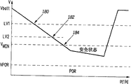
Accompanying drawing 2 is depicted as the accompanying drawing according to the method that enters and withdraw from safe condition of the first embodiment of the present invention.When Vbatt began to descend, because the cause of electric power battery faint or that be removed (Vbatt provides by capacitor 104 here), LVD1 110 detected Vbatt and when reaches about LV1, and this illustrates to put 180 in accompanying drawing 2.In case reach a little 180, if MCU 102 just operates under stop mode, then LVD2 116 periodically starts to provide accurate low-voltage to detect.
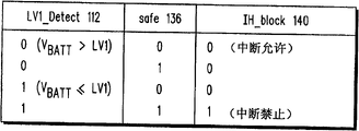
For example, turn back to accompanying drawing 1, PWU start unit 120 starts PWU 124 based on LV1_Detect 112, safe 136 and STOP 132.That is, when the value of LV1_Detect 112, safe 136 and STOP 132 was shown in the truth table of accompanying drawing 5, PWU start unit 120 was claimed PWU_en 122 (to start PWU 124).That is, as shown in Figure 5, only when claiming LV1_Detect 112, claim STOP 132 and not claiming safe 136, claim PWU_en122.That is, detect Vbatt at LVD1 110 and (therefore claim LV1_Detect112) under LV1 the time, MCU 102 is in stop mode (claiming STOP 132), and MCU 102 is not in a safe condition (not claiming safe 136), starts PWU 124.Note, in the combination of all other of the value of LV1_Detect112, safe 136 and STOP 132, do not claim PWU_en122 so that do not start PWU 124.
PWU 124 provides wakeup 126 to LVD2 start unit 128.In one embodiment, wakeup 126 is the recurrent pulses that are used for periodically starting by LVD2 start unit 128 LVD2116.That is, LVD2 start unit 128 receive wakeup 126 and STOP 132 and with LVD2_en 130 offer LVD2116 (and voltage regulator 114, if present).When claiming LVD2_en 130, LVD2 116 starts and monitoring Vbatt is higher than with definite Vbatt or be lower than LV2.(replacedly, as indicated above, if there is voltage regulator 114, LVD2 116 can monitor Vreg, and it can be substantially equal to Vbatt to determine Vbatt and be higher than or be lower than LV2 in this case).LVD2 start unit 128 is according to operating at the truth table shown in the accompanying drawing 4.Therefore, (when not claiming STOP132) claims LVD2_en 130 in the time of in operational mode, therefore starts LVD2 116.Yet, when stop mode, (claim STOP 132), only when claiming wakeup 126, claim LVD2_en 130.Like this, in the stop mode process and when Vbatt is between LV1 and the LV2, LVD2 116 periodically starts so that consume minimal power by wakeup 126.
Turn back to the curve map of accompanying drawing 2, along with Vbatt continue to descend, because the cause of faint battery of electric power or the battery that is removed, when LVD2 116 monitoring Vbatt reach LV2, and LV2 illustrates by putting 182 in accompanying drawing 2.Notice that if MCU 102 operates, then LVD2 116 detects the Vbatt that reaches LV2 at the one-period of determining by wakeup 126 in the time under stop mode.Yet if MCU 102 operates under operational mode, LVD2 116 always starts (that is, when falling tone claims STOP 132, always claim LVD2_en 130, and have nothing to do with wakeup 126), and detects the Vbatt that reaches LV2.As indicated above, LVD2116 detects more accurately when Vbatt arrives LV2 the Vbatt that arrives LV1 except LVD1 110 detects.In case reach LV2, LVD2 116 claims LV2_interrupt 118.Notice that in one embodiment, LV2_interrupt 118 specifies the highest priority to admit by interrupt handler 142 immediately to guarantee it.Therefore, in this embodiment, in case claim LV2_interrupt 118, then interrupt handler 142 allows CPU 160 to serve LVD2116 interruption undetermined.Being used to serve interrupt service routine that LVD2 116 interrupts can comprise instruction and close safely to allow MCU 102.For example, interrupt service routine can be preserved any required information (comprising status information) storer 158, and signal can be saved in the external unit 166 etc.
Because near MCU 102 just operation Vmin now (being that Vbatt is just near the place of Vmin), so MCU 102 places safe condition should or arrive it before Vmin the time.In one embodiment, interrupt service routine can comprise with safe bit register 134 be set to 1 with the indication entered safe condition instruction.Note, when safe bit register 134 is set up, claim that safe 136 admits interruption undetermined or future with disabled interrupt processor 142.For example, with reference to the accompanying drawings 1, the response of IH control module 138 control 142 pairs of outsides of interrupt handler and internal interrupt.IH control module 138 receives LV1_Detect 112 and safe 136 and claims selectively as passing through the IH_block 140 shown in the truth table of accompanying drawing 3.For example, only claim LV1_Detect 112 and safe 136 both the time, IH control module 138 is claimed IH_block 140.When claiming IH_block 140, forbid or stop interrupt handler 142 to admit interruption from external interrupt 144 or internal interrupt 146.Therefore, in one embodiment, each interruption have externally interrupt 144 or internal interrupt 146 in the look-at-me of correspondence.Each look-at-me can enter the AND door by 140 independent preventions of IH_block by moving each look-at-me and IH_block 140.Replacedly, other startup OR circuit can be used for forbidding being input to interrupt handler 142.In a kind of variant embodiment, IH_block 140 can be used for making interrupt handler 142 all or part of stop realizing the prevention of interrupting or to forbid.In an embodiment again, the output gating that IH_block 140 can be by interrupt handler 142 is to realize the prevention of interrupting or to forbid.
Notice that in a kind of variant embodiment, safe 136 can implement in a different manner.For example, response LVD2 116 detects the Vbatt that reaches LV2 and (in certain embodiments, Vreg), can automatically claim safe 136 (rather than passing through interrupt service routine).Be also noted that safe bit register 134 can be thought in MCU 102 Anywhere.
Turn back to accompanying drawing 2, MCU 102 remains on safe condition, rises on the LV1 once more up to Vbatt.That is, when inserting new battery, perhaps when current battery was recharged, Vbatt rose on the LV1 once more, and safe condition withdraws from and safe bit register 134 resets to 0 on this aspect, so falling tone claims safe 136.Therefore MCU 102 can admit to interrupt once more, and can withdraw from stop mode safely and turn back to operational mode.Replacedly, in case Vbatt rises on the LV1, safe bit register 134 does not reset.In this embodiment, after waking MCU 102 up or some the point on, safe bit register can be removed by the user.
In an embodiment of the present invention, LVD1 110 also can be used for detecting Vbatt and when drops to power-on-reset voltage (VPOR) (as shown in Figure 2) less than Vmin.When Vbatt reached VPOR, RAM and internal logic states were destroyed wholly or in part usually.If change or to battery charge before Vbatt reach VPOR, then because data corruption, in case change battery or, then need initialization MCU 102 to battery charge.Be also noted that in certain embodiments, reset interrupt or power-on-reset interrupt may have than above-described LVD2 116 interrupts higher priority.
Accompanying drawing 6 is depicted as the synoptic diagram of a kind of embodiment of the LVD circuit 200 of the LVD1 110 that can be used for accompanying drawing 1.LVD circuit 200 comprises comparer 212, transistor 208,204 and 206 and current source 202 and 210.Current source 202 has the first terminal that is coupled to Vbatt and is coupled to the positive input (Vref) of comparer 212 and second terminal of first galvanic electrode of transistor 204.Current source 202 provides electric current I ref for the positive input of comparer 212 and first galvanic electrode of transistor 204.Second galvanic electrode of transistor 204 is coupled to the control electrode of transistor 204 and first galvanic electrode of transistor 206.Second galvanic electrode of the control electrode of transistor 206 and transistor 206 is coupled to each other, and is coupled to second terminal and the ground contacts of current source 210.First galvanic electrode of transistor 208 is coupled to Vbatt and control electrode, and second control electrode of transistor 208 is coupled to the negative input (Vcomp) of comparer 212 and the first terminal of current source 210.Current source 210 provides electric current I comp.The output of comparer 212 provides LV1_Detect 112.Notice that in an illustrated embodiment, transistor 204 and 208 is p-type mosfet transistors, transistor 206 is bipolar transistors.Yet, in variant embodiment, also can use the transistor of other type, different circuit structures can be used for providing LV1_Detect 112.
In operation, current source 202 is used for transistor 206 and 204 bias voltages to produce reference voltage Vref.The value of Vref equals threshold voltage (Vtp) sum of the base stage of transistor 206 to emitter voltage (Vbe) and transistor 204.Current source 210 is used for transistor 208 bias voltages are equaled with generation the Vcomp of the threshold voltage (Vtp) that Vbatt deducts transistor 208.Relation by comparer 212 monitoring Vcomp and Vref.When Vcomp is higher than Vref, the output of comparer 212 lower (falling tone claims in the present embodiment).As long as Vbatt descends to such an extent that enough lowly be less than or equal to Vref so that Vcomp becomes, then comparer output is from the low height that switches to, the detection of indication low-voltage state.Therefore, in this, claim LV1_Detect 112, indication Vbatt has reached LV1.
The current source 202 and 210 that uses in LVD circuit 200 has very low circuit values.For this reason, for the low-voltage measuring ability, LVD circuit 200 has than the common required lower noise immunity of noise immunity of this circuit.Yet, in one embodiment, the operation of LVD circuit 200 only MCU 102 be in the low-power stop mode and all clocks important when all stopping.The reference voltage Vref that produces by LVD circuit 200 can be highly inaccurate, because the cause of the deviation aspect processing parameter and temperature.Yet, produce interruption so that therefore system closing does not require highly accurate, as indicated above because this circuit is not used in to MCU 102.That is, LVD1 110 only is used for starting under suitable condition accurate more LVD2 116 and MCU 102 is remained on low power safe state, externally (passes through Vbatt) up to enough voltage and recovers to allow MCU 102 beginnings to handle once more.
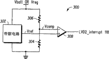
Accompanying drawing 7 is depicted as the synoptic diagram of a kind of embodiment of the LVD circuit 300 of the LVD2 116 that can be used for accompanying drawing 1.LVD circuit 300 comprises band-gap circuit 302, resistance 306 and 304 and comparer 308.Vbatt (if perhaps there is voltage regulator 114, Vref) is coupled to the first terminal of band-gap circuit 302 and the first terminal of resistance 306.Second terminal of band-gap circuit 302 is coupled to the positive input of comparer 308 so that Vref to be provided, and the 3rd terminal of band-gap circuit 302 is coupled to the first terminal and the ground contacts of resistance 304.Second terminal of resistance 306 is coupled to the negative input of second terminal and the comparer 308 of resistance 304.Comparer 308 has the output that LV2_interrupt 118 is provided.Notice that different embodiment can use different circuit structures so that LV2_interrupt 118 to be provided.
Though described the last stakes invention with reference to specific conductivity type or polarity of voltage, what it should be understood by one skilled in the art that is that conductivity type and polarity of voltage can be reverse.
In aforesaid instructions, reference example has been described the present invention.Yet, it will be appreciated by one skilled in the art that under the prerequisite of the scope of in not breaking away from, setting forth of the present invention and can make various improvement and change as claim below.For example, calcspar can have except shown in calcspar different squares, and can have more or less square or differently be provided with.In addition, some square can make up.For example, a kind of variant embodiment can become the function combinations of LVD1 110 and LVD2 116 single LVD system, and this list LVD system can operate in high power and low-power mode and provide a kind of indication under Vbatt drops to LV1 the time and another kind of indication is provided under Vbatt drops to LV2 the time.Therefore, instructions and accompanying drawing should be counted as illustrative and not restrictive, and all this improvement are all wished to be included in the scope of the present invention.
The scheme of above having described benefit of the present invention, other advantage and having dealt with problems with reference to certain embodiments.Yet, these benefits, advantage, the scheme of dealing with problems and may make the clearer and more definite any element of any benefit, advantage or scheme should not be interpreted as feature key, desired or basic or the element of any or all of claim.Just as used herein, term " comprises " or any other similar term all is that nonexcludability comprises, therefore the process, method, object or the equipment that comprise the element tabulation not only comprise these elements, but can also comprise except this process, method, object or equipment other element intrinsic or that do not listed clearly.
Claims (13)
1. an integrated circuit (100) comprising:
Power supply lead wire (109) from the power supply received power;
First voltage detecting circuit (110) has output, and first voltage detection signal is provided, and when the voltage level that is used to refer to power supply lead wire is lower than first voltage level;
Second voltage detecting circuit (116) has output, and second voltage detection signal is provided, and when the voltage level that is used to refer to power supply lead wire is lower than second voltage level, and this second voltage level is lower than first voltage level;
CPU (central processing unit) (160), this CPU (central processing unit) are configured to from the power power supply that receives by power supply lead wire;
Operatively be coupled to the interrupt handler (142) of CPU (central processing unit), this interrupt handler response comprises one group of interruption of at least one interruption;
Interrupt handler control circuit (138), be used to control interrupt handler to comprising one group of response of interrupting of at least one interruption, this interrupt handler control circuit responds first voltage detection signal and responds first signal with first signal condition, this first signal condition indicates the voltage level of power supply lead wire indicated as second voltage detection signal at least, be reduced under second voltage level, wherein when first signal was in first signal condition, response comprised described one group of interruption of at least one interruption when interrupt handler control circuit startup interrupt handler was higher than first voltage level with the voltage level at first voltage detection signal indication power supply lead wire.
2. the described integrated circuit of claim 1, wherein first signal is set to first signal condition by the processing operation of CPU (central processing unit).
3. the described integrated circuit of claim 2, wherein:
Interrupt handler is coupled in the output of second voltage detecting circuit,
Wherein indicate second voltage detection signal of voltage level under second voltage level of power supply lead wire to produce interruption;
CPU (central processing unit) carry out to handle operation with the interruption that responds voltage level at second voltage detection signal indication power supply lead wire at least and produce under second voltage level time with first signal sets to first signal condition.
4. the described integrated circuit of claim 1, wherein integrated circuit has the low-power stop mode, and wherein second voltage detecting circuit stops to provide second voltage detection signal when integrated circuit is in the low-power stop mode.
5. the described integrated circuit of claim 4 further comprises:
The voltage level that wake-up circuit, the output of this wake-up circuit are in low-power stop mode and first voltage detection signal indication power supply lead wire at integrated circuit at least makes second voltage detecting circuit that second voltage detection signal is provided when being lower than first voltage level.
6. the described integrated circuit of claim 1, wherein the interrupt handler control circuit enters interrupt handler by at least one look-at-me of gating (148) and controls interrupt handler to comprising described one group of response of interrupting of at least one interruption.
7. system that can carry out the battery power-on servicing comprises the described integrated circuit of claim 1, and further comprises:
Be coupled to power supply lead wire to give the battery of power supply lead wire transmission power; With
Operatively be coupled to the external unit of integrated circuit by at least one signal wire pin of integrated circuit.
8. integrated circuit comprises:
Power supply lead wire (109) from the power supply received power;
First voltage detecting circuit (110) has output, and first voltage detection signal is provided, and when the voltage level that is used to refer to power supply lead wire is lower than first voltage level;
Second voltage detecting circuit (116) has output, and second voltage detection signal is provided, and when the voltage level that is used to refer to power supply lead wire is lower than second voltage level, and this second voltage level is lower than first voltage level;
Wake-up circuit (124), the output of this wake-up circuit (126) starts second voltage detecting circuit so that second voltage detection signal to be provided when the voltage level of first voltage detection signal indication power supply lead wire is lower than first voltage level.
9. the described integrated circuit of claim 8 further comprises:
Interrupt handler (142), this interrupt handler response comprises one group of interruption of at least one interruption;
Interrupt handler control circuit (138), be used to control interrupt handler to comprising one group of response of interrupting of at least one interruption, this interrupt handler control circuit responds first voltage detection signal and responds first signal with first signal condition, first signal condition indicates the voltage level of power supply lead wire indicated as second voltage detection signal at least, be reduced under second voltage level, wherein when first signal was in first signal condition, response comprised described one group of interruption of at least one interruption when interrupt handler control circuit startup interrupt handler was higher than first voltage level with the voltage level at first voltage detection signal indication power supply lead wire.
10. the described integrated circuit of claim 8, wherein when the voltage level of at least the first voltage detection signal indication power supply lead wire was lower than first voltage level and integrated circuit and is in the low-power stop mode, wake-up circuit started second voltage detecting circuit so that second voltage detection signal to be provided.
11. the described integrated circuit of claim 8, wherein wake-up circuit is the periodic wakeup circuit, wherein when the voltage level of at least the first voltage detection signal indication power supply lead wire was lower than first voltage level, this output provided cyclical signal to start second voltage detecting circuit so that second voltage detection signal to be provided.
12. the described integrated circuit of claim 8 further comprises:
First signal, this first signal has first signal condition, and this first signal condition indicates the voltage level of power supply lead wire to be reduced to as passing through under the second indicated voltage level of second voltage detection signal at least;
Wherein when the voltage level of at least the first voltage detection signal indication power supply lead wire was lower than first voltage level and first signal and is in the secondary signal state that is different from first signal condition, the output of wake-up circuit started second voltage detecting circuit so that second voltage detection signal to be provided.
13. an integrated circuit comprises:
Power supply lead wire (109) from the power supply received power;
CPU (central processing unit) (160), this CPU (central processing unit) are configured to from the power power supply that receives by power supply lead wire;
Voltage detecting system, this voltage detecting system is configured to provide the voltage level of power supply lead wire to be reduced to the indication of first under first voltage level (118), and be configured to provide the voltage level of power supply lead wire to rise to the indication of second on second voltage level (112), wherein first voltage level is lower than second voltage level;
Operatively be coupled to the interrupt handler (142) of CPU (central processing unit), this interrupt handler response comprises one group of interruption of at least one interruption;
The interrupt handler control circuit, be used to control interrupt handler to comprising one group of response of interrupting of at least one interruption, wherein when first signal (136) is in first signal condition, the voltage level of this first signal condition indication power supply lead wire is indicated as first indication, be reduced under first voltage level, this interrupt handler control circuit response second indication starts interrupt handler comprises at least one interruption with response described one group of interruption.
Applications Claiming Priority (2)
| Application Number | Priority Date | Filing Date | Title |
|---|---|---|---|
| US10/292,323 | 2002-11-12 | ||
| US10/292,323 US7293188B2 (en) | 2002-11-12 | 2002-11-12 | Low voltage detection system |
Publications (2)
| Publication Number | Publication Date |
|---|---|
| CN1695103A CN1695103A (en) | 2005-11-09 |
| CN100559326C true CN100559326C (en) | 2009-11-11 |
Family
ID=32229432
Family Applications (1)
| Application Number | Title | Priority Date | Filing Date |
|---|---|---|---|
| CNB038250209A Expired - Fee Related CN100559326C (en) | 2002-11-12 | 2003-09-30 | Low voltage detection system |
Country Status (7)
| Country | Link |
|---|---|
| US (1) | US7293188B2 (en) |
| JP (1) | JP4322810B2 (en) |
| KR (1) | KR101031117B1 (en) |
| CN (1) | CN100559326C (en) |
| AU (1) | AU2003275307A1 (en) |
| TW (1) | TWI331276B (en) |
| WO (1) | WO2004044719A2 (en) |
Families Citing this family (23)
| Publication number | Priority date | Publication date | Assignee | Title |
|---|---|---|---|---|
| JP2004078717A (en) * | 2002-08-21 | 2004-03-11 | Matsushita Electric Ind Co Ltd | Cell library database, and integrated circuit timing verification system and voltage resistance verification system using cell library database |
| US7349190B1 (en) | 2003-12-22 | 2008-03-25 | Cypress Semiconductor Corp. | Resistor-less accurate low voltage detect circuit and method for detecting a low voltage condition |
| CN100362452C (en) * | 2005-05-27 | 2008-01-16 | 佛山市顺德区顺达电脑厂有限公司 | User operation blocking device and method |
| CN100362451C (en) * | 2005-05-27 | 2008-01-16 | 佛山市顺德区顺达电脑厂有限公司 | User operation block device and method |
| CN100444490C (en) * | 2005-07-11 | 2008-12-17 | 佛山市顺德区顺达电脑厂有限公司 | Operation blocker and blocking method for user |
| US7629769B2 (en) * | 2006-03-10 | 2009-12-08 | Atmel Corporation | Power surge filtering in over-current and short circuit protection |
| JP4715760B2 (en) * | 2006-07-28 | 2011-07-06 | 株式会社デンソー | Microcomputer and control system |
| KR100897767B1 (en) * | 2007-02-07 | 2009-05-15 | 삼성전자주식회사 | Method and MCU capable of further preserving and holding data |
| US7917328B2 (en) * | 2008-08-20 | 2011-03-29 | International Business Machines Corporation | Tracking thermal mini-cycle stress |
| US8174382B2 (en) * | 2008-11-21 | 2012-05-08 | Mahle International Gmbh | Diagnostic system having a wake-up circuit |
| US8305068B2 (en) * | 2009-11-25 | 2012-11-06 | Freescale Semiconductor, Inc. | Voltage reference circuit |
| US8330502B2 (en) * | 2009-11-25 | 2012-12-11 | Freescale Semiconductor, Inc. | Systems and methods for detecting interference in an integrated circuit |
| JP2011210152A (en) * | 2010-03-30 | 2011-10-20 | Renesas Electronics Corp | Microcomputer |
| US8330526B2 (en) * | 2010-07-15 | 2012-12-11 | Freescale Semiconductor, Inc. | Low voltage detector |
| US8924604B2 (en) * | 2011-09-26 | 2014-12-30 | Belkin International, Inc. | Systems and methods for data compression and feature extraction for the purpose of disaggregating loads on an electrical network |
| US8907807B2 (en) * | 2013-03-15 | 2014-12-09 | Oplink Communications, Inc. | Security system power management |
| WO2014202692A2 (en) * | 2013-06-21 | 2014-12-24 | Fujitsu Technology Solutions Intellectual Property Gmbh | Computer system and overload protection circuit |
| US9141177B1 (en) | 2014-03-21 | 2015-09-22 | Western Digital Technologies, Inc. | Data storage device employing glitch compensation for power loss detection |
| US9047932B1 (en) | 2014-03-21 | 2015-06-02 | Western Digital Technologies, Inc. | Data storage device adjusting a power loss threshold based on samples of supply voltage |
| US9696789B2 (en) * | 2014-08-18 | 2017-07-04 | Xilinx, Inc. | Sub-system power management control |
| JP7295993B2 (en) | 2017-10-26 | 2023-06-21 | 株式会社イトーキ | Desk with adjustable top plate |
| JP7153791B2 (en) * | 2018-09-21 | 2022-10-14 | 長江存儲科技有限責任公司 | Voltage detection system |
| JP6886545B1 (en) | 2020-05-07 | 2021-06-16 | ウィンボンド エレクトロニクス コーポレーション | Power-down detection circuit and semiconductor storage device |
Family Cites Families (10)
| Publication number | Priority date | Publication date | Assignee | Title |
|---|---|---|---|---|
| US5203000A (en) * | 1988-12-09 | 1993-04-13 | Dallas Semiconductor Corp. | Power-up reset conditioned on direction of voltage change |
| US5241680A (en) * | 1989-06-12 | 1993-08-31 | Grid Systems Corporation | Low-power, standby mode computer |
| US5428252A (en) * | 1992-01-03 | 1995-06-27 | Zilog, Inc. | Power supply interruption detection and response system for a microcontroller |
| US5423045A (en) * | 1992-04-15 | 1995-06-06 | International Business Machines Corporation | System for distributed power management in portable computers |
| DE4314533C1 (en) * | 1993-05-03 | 1994-05-19 | Siemens Ag | Microprocessor battery-supply voltage monitoring circuit - has low-voltage detector for generating reset when supply is between first and second low voltages, and comparator for generating signal when supply is above higher voltage to operate processor |
| EP0777895B1 (en) * | 1994-08-26 | 2003-10-08 | Interlogix, Inc. | Self-contained, self-adjusting smoke detector and method of operating it |
| JPH11119872A (en) * | 1997-10-13 | 1999-04-30 | Sanyo Electric Co Ltd | Power source voltage detection circuit |
| EP1102158B1 (en) * | 1999-11-22 | 2012-08-08 | EM Microelectronic-Marin SA | Apparatus and procedure for controlling the operation of an electronic system in a "grey zone" |
| JP2001188689A (en) * | 2000-01-04 | 2001-07-10 | Mitsubishi Electric Corp | Data processor |
| KR100450963B1 (en) * | 2001-08-16 | 2004-10-02 | 삼성전자주식회사 | Method and device for handling dying gasp in customer premise equipment of digital subscriber line |
-
2002
- 2002-11-12 US US10/292,323 patent/US7293188B2/en active Active
-
2003
- 2003-09-30 KR KR1020057008523A patent/KR101031117B1/en active IP Right Grant
- 2003-09-30 WO PCT/US2003/030864 patent/WO2004044719A2/en active Application Filing
- 2003-09-30 CN CNB038250209A patent/CN100559326C/en not_active Expired - Fee Related
- 2003-09-30 AU AU2003275307A patent/AU2003275307A1/en not_active Abandoned
- 2003-09-30 JP JP2004551487A patent/JP4322810B2/en not_active Expired - Fee Related
- 2003-10-15 TW TW092128565A patent/TWI331276B/en not_active IP Right Cessation
Also Published As
| Publication number | Publication date |
|---|---|
| TW200428193A (en) | 2004-12-16 |
| JP2006506617A (en) | 2006-02-23 |
| KR101031117B1 (en) | 2011-04-27 |
| AU2003275307A8 (en) | 2004-06-03 |
| CN1695103A (en) | 2005-11-09 |
| JP4322810B2 (en) | 2009-09-02 |
| WO2004044719A3 (en) | 2004-09-02 |
| US7293188B2 (en) | 2007-11-06 |
| US20040093531A1 (en) | 2004-05-13 |
| AU2003275307A1 (en) | 2004-06-03 |
| WO2004044719A2 (en) | 2004-05-27 |
| TWI331276B (en) | 2010-10-01 |
| KR20050075397A (en) | 2005-07-20 |
Similar Documents
| Publication | Publication Date | Title |
|---|---|---|
| CN100559326C (en) | Low voltage detection system | |
| KR920002245B1 (en) | Portable computer operated by batteries | |
| US7876144B2 (en) | Start-up circuit and start-up method | |
| US6714016B2 (en) | Method for displaying information concerning power consumption and electronic device | |
| US4984185A (en) | Portable computer having a battery voltage detecting circuit | |
| EP3432119B1 (en) | Devices and methods for power sequence detection | |
| TW201315090A (en) | Controllers, systems and methods for controlling battery management systems | |
| US8278932B2 (en) | Method and detector for determining a state of a switch | |
| CN114072984A (en) | Battery management apparatus | |
| CN100356684C (en) | IC apparatus for monitoring power supply | |
| US5619156A (en) | Low voltage inhibit circuit and integrated circuit using same | |
| CN113495605A (en) | Power saving power architecture for integrated circuits | |
| CN110928392A (en) | Power supply control device and electronic apparatus | |
| CN209766595U (en) | overlength standby device | |
| CN112649724A (en) | Power failure detection circuit and method and MCU chip | |
| CN105098854B (en) | Charging method and electronic device | |
| CN211349294U (en) | Power supply control device and electronic apparatus | |
| CN103633973A (en) | A power supply reset circuit with zero standby current consumption | |
| CN218829149U (en) | Battery protection circuit | |
| CN112198349A (en) | Electric meter | |
| CN219018791U (en) | Time-sharing multiplexing circuit for key detection and level detection | |
| CN220173216U (en) | Reset circuit and electronic equipment | |
| CN216872087U (en) | Low-power consumption wake-up circuit | |
| CN117666742B (en) | Server management engine recovery circuit | |
| CN218603202U (en) | Wake-up circuit, battery device and electronic equipment |
Legal Events
| Date | Code | Title | Description |
|---|---|---|---|
| C06 | Publication | ||
| PB01 | Publication | ||
| C10 | Entry into substantive examination | ||
| SE01 | Entry into force of request for substantive examination | ||
| C14 | Grant of patent or utility model | ||
| GR01 | Patent grant | ||
| CP01 | Change in the name or title of a patent holder | ||
| CP01 | Change in the name or title of a patent holder |
Address after: Texas in the United States Patentee after: NXP USA, Inc. Address before: Texas in the United States Patentee before: FREESCALE SEMICONDUCTOR, Inc. |
|
| CF01 | Termination of patent right due to non-payment of annual fee | ||
| CF01 | Termination of patent right due to non-payment of annual fee |
Granted publication date: 20091111 Termination date: 20210930 |