EP0408002B1 - A programmable semiconductor memory apparatus - Google Patents
A programmable semiconductor memory apparatus Download PDFInfo
- Publication number
- EP0408002B1 EP0408002B1 EP90113258A EP90113258A EP0408002B1 EP 0408002 B1 EP0408002 B1 EP 0408002B1 EP 90113258 A EP90113258 A EP 90113258A EP 90113258 A EP90113258 A EP 90113258A EP 0408002 B1 EP0408002 B1 EP 0408002B1
- Authority
- EP
- European Patent Office
- Prior art keywords
- identifying code
- semiconductor memory
- bit lines
- spare
- programmable semiconductor
- Prior art date
- Legal status (The legal status is an assumption and is not a legal conclusion. Google has not performed a legal analysis and makes no representation as to the accuracy of the status listed.)
- Expired - Lifetime
Links
Images

Classifications
-
- G—PHYSICS
- G11—INFORMATION STORAGE
- G11C—STATIC STORES
- G11C17/00—Read-only memories programmable only once; Semi-permanent stores, e.g. manually-replaceable information cards
-
- G—PHYSICS
- G11—INFORMATION STORAGE
- G11C—STATIC STORES
- G11C5/00—Details of stores covered by group G11C11/00
-
- G—PHYSICS
- G06—COMPUTING; CALCULATING OR COUNTING
- G06F—ELECTRIC DIGITAL DATA PROCESSING
- G06F11/00—Error detection; Error correction; Monitoring
- G06F11/006—Identification
-
- G—PHYSICS
- G11—INFORMATION STORAGE
- G11C—STATIC STORES
- G11C16/00—Erasable programmable read-only memories
- G11C16/02—Erasable programmable read-only memories electrically programmable
- G11C16/06—Auxiliary circuits, e.g. for writing into memory
- G11C16/08—Address circuits; Decoders; Word-line control circuits
-
- G—PHYSICS
- G11—INFORMATION STORAGE
- G11C—STATIC STORES
- G11C16/00—Erasable programmable read-only memories
- G11C16/02—Erasable programmable read-only memories electrically programmable
- G11C16/06—Auxiliary circuits, e.g. for writing into memory
- G11C16/10—Programming or data input circuits
- G11C16/20—Initialising; Data preset; Chip identification
-
- G—PHYSICS
- G11—INFORMATION STORAGE
- G11C—STATIC STORES
- G11C16/00—Erasable programmable read-only memories
- G11C16/02—Erasable programmable read-only memories electrically programmable
- G11C16/06—Auxiliary circuits, e.g. for writing into memory
- G11C16/24—Bit-line control circuits
Definitions
- the present invention relates to a programmable semiconductor memory apparatus (called an RWM: Read/Write Memory) and more particularly to an RWM with a circuit for storing a device identifying code.
- an RWM Read/Write Memory
- An RWM can be generally divided into a RAM (Random Access Memory) and a ROM (Read Only Memory).
- a programmable ROM corresponds to an RWM.
- a programmable ROM is classified from the viewpoint of structure into a bipolar-type, a FAMOS (Floating-gate Avalanche Injection MOS) or an MNOS (Metal Nitride Oxide Semiconductor), and classified from the viewpoint of whether it is applied into a fuse ROM (programmable ROM), an EP-ROM(Erasable Programmable ROM), an EEP-ROM (Electrically Erasable and Programmable ROM), or an EA-ROM (Electrically Alterable ROM).
- An RWM is forwarded from the manufacturer in a blank state, i.e., in a state where the data is not written, the user-side writes data by ROM writer.
- a ROM writer has a function of automatically setting a condition for writing data into an RWM device. Therefore, a circuit for storing a self device identifying code and enabling the self device identifying code to be read upon writing data into RWM is generally provided on the device side.
- the self device identifying code represents the conditions for writing data into an RWM such as the name of a manufacturer memory capacity, the kind of writing algorithm and chip revision of the RWM.
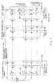
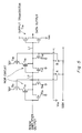
- Figure 1 shows the structure of a prior art RWM circuit for explaining the operation of the RWM.
- An RWM generally comprises a first memory cell array 1 to a k-th memory cell array 3, and data sense circuits 4. More precisely, a RWM comprises bit lines B 1 to B m , word lines W 1 to W n and W c , memory transistors Q 11 to Q mn , bit line selection transistors Q 1s to Q ms , device identifying code storing transistors Q 1c to Q kc and bus lines B u1 to B uk .
- an address signal is produced to select one word line (for example W 1 ) and one bit line (for example B 1 ) to select a predetermined memory transistor Q 11 , and data is written by applying an "H" signal or an "L” signal to memory transistor circuit Q 11 .
- a predetermined memory transistor Q 11 is selected by the same operation as above, thereby outputting the stored data.
- the device identifying code is stored in device identifying code storing transistors Q 1c to Q kc connected to the bit line.
- a device identifying code storing transistors Q 1c to Q kc is provided for respective memory cell arrays and as k device identifying code storing transistors Q 1c to Q kc are used, the number of device identifying codes comprises k bits.
- the exclusive word line W c may be selected to enable the device identifying code to be read out. This makes a device of this type easy to pattern and thus it is widely used.
- a redundant bit line is generally provided to increase yield.
- a redundant bit line is provided by preparing several spare bit lines in the memory.
- a spare bit line is selected when an address signal selecting the faulty portion enters the memory.
- a device containing a fault can be used as if it were fault-free.
- a redundant bit line is embodied, there is always a possibility of replacing a discretional bit line by a spare bit line. In this case the replaced bit line is not used thereafter.
- the device identifying code storing transistor Q ic When the device identifying code storing transistor Q ic is connected to the replaced bit line, an element of the device identifying code stored in the device identifying code storing transistor Q ic , for example, the i-th element of the k-bit code, is lacking and thus cannot be read out. This prevents the device identifying code from performing an effective function. Therefore, when the bit line redundancy is embodied, the type with the device identifying code stored in the device identifying code storing transistor connected to the bit line cannot be used.
- Document US-A-4,055,802 discloses a configuration with the purpose to provide a technology by which a circuit configuration can be electrically identified.
- a cathode of a diode is connected to respective input lines (or output lines) of a chip in a ROM and an electrical switch is provided at an anode side of the diode for switching over the coupling to ground or an emitter of the transistor.
- an electrical interrogation signal is applied to the input lines an unique pattern appears representative of the particular circuit.
- a semiconductor memory having identifying code storing means connected to input lines or output lines.
- An object of the present invention is to provide an improved RWM capable of storing the device identifying code to enable the device identifying code to be easily read out even when a bit line redundancy is adopted.
- this object is achieved by a programmable semiconductor memory apparatus according to claim 1.
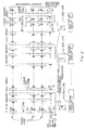
- Figure 2 shows the first embodiment of the present invention.
- the same parts as those in the prior art shown in Figure 1 are provided with the same reference numbers, and detailed explanations of such parts are omitted.
- a programmable semiconductor memory apparatus comprises memory cell arrays 1,2,3, data sense circuits 4 for writing data into and reading data from said memory cell arrays 1,2,3, bus lines B u1 to B uk connected to a common node of a plurality of bit lines B 1 to B m , B s1 to B sj forming the memory cell arrays 1,2,3, and a means for storing an identifying code for identifying said programmable semiconductor memory device being coupled to said bus lines B u1 to B uk , thereby enabling said identifying code to be read externally.
- a discretional spare bit line is selected in place of a faulty bit line.
- the device identifying code is not stored in device identifying code storing transistors Q 1c to Q kc connected to the bit line as in the case of the prior art RWM, but in a memory circuit connected to bus lines B u1 to B uk provided between the common node of the bit lines B 1 to B m and B s1 to B sj and the data sense circuits 4. Therefore, even if one of the faulty bit lines is disposed of, and instead any spare bit line is selected, a device identifying code can be correctly read out without being affected.
- a device identifying code is programmed in device identifying code storing transistors Q 1D to Q kD upon the manufacturing of an RWM.
- Device identifying code storing transistors Q 1D to Q kD are turned on when an (H) signal more than threshold voltage V TH is applied to the gates G 1D to G kD thereof and they are turned off when an (L) signal less than the threshold voltage V TH is applied to G 1D to G kD thereof.
- the device identifying storing transistors Q 1D to Q kD are of the enhancement type.
- Device identifying code storing transistors Q 1D to Q kD are of the type having a threshold voltage V TH changed by an electric operation.
- the transistors Q 1D to Q kD are formed such that in accordance with an electrical operation, they have two threshold voltages comprising a voltage V 1 which is higher than the source voltage Vcc and a voltage V 2 which is lower than the source voltage Vcc. Codes determined as being logic “0” or “1” depending on voltages V 1 and V 2 are provided for respective device identifying code storing transistors Q 1D to Q kD .
- the power source voltage Vcc is applied to gates G 1D to G kD , the transistor with the threshold voltage of V 1 is turned off and the transistor with the threshold voltage V 2 is turned on.
- k bits of device identifying code can be stored by determining that logic “0" corresponds to voltage V 1 and logic “1” corresponds to voltage V 2 , depending on whether the threshold voltage of the transistors Q 1D to Q kD is determined as being V 1 or V 2 .
- k bits of device identifying code may be stored by determining that logic "1” corresponds to voltage V 1 and logic "0" corresponds to voltage V 2 .
- the device identifying code can be programmed based on threshold voltages V 1 and V 2 of device identifying storing transistors Q 1D to Q kD .
- Address signals A Do to A Dn and signature signal SGH ⁇ are applied to NAND circuit 11.
- the output of NAND circuit 11 is applied to gates G 1s to G ms of bit line selecting transistors Q 1s to Q ms and gates G ss to G sj of spare bit line selecting transistors Q ss to Q sj through inverter 12.
- an "L" signal is applied to all the gates of G 1s to G ms of bit line selecting transistors Q 1s to Q ms and gates G ss to G sj of spare bit line selecting transistors Q ss to Q sj from inverter 12, as signature singal SGH is turned high.
- source voltage V cc is applied to gates G 1D to G kD of device identifying code storing transistors Q 1D to Q kD and thus the device identifying code can be read out.
- NMOS transistors may be provided between the common nodes of bit lines and a spare bit line forming memory cell arrays 1, 2 and 3 and drains of NMOS transistors Q 1D to Q kD .
- the signature signal SGH ⁇ may be applied to gates of the NMOS transistors to read the device idintifying code.
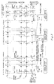
- Figure 3 shows the second embodiment of the present invention. This embodiment is different from that in Figure 2 in that device identifying storing transistors Q 1E to Q kE are provided in place of device identifying code storing transistors Q 1D to Q kD shown in Figure 2, and electric switching means S 1E to S kE are provided on a line connecting device identifying code storing transistors Q 1E to Q kE and bus lines B u1 to B uk .
- Device identifying code storing transistor Q 1E to Q kE are different from device identifying code storing transistors Q 1D to Q kD in that the threshold voltage V TH may not be variable in accordance with an electric operation.
- Transistors Q 1D to Q kD turn on when an (H) signal is applied to gates G 1E to G kE .
- the threshold voltage V TH is made less than or equal to power source voltage Vcc.
- the device identifying code is programmed by using electric switching means S 1E to S kE .
- Electric switching means S 1E to S kE may be of the so-called fuse type which are conductive before programming but are melted to be cut out or made nonconductive by an application of a current upon programming.
- Electric switching means S 1E to S kE may also be of the type which are nonconductive before programming but, are made conductive by an application of a current upon programming when connected through melting. It is possible to program the device identifying code by determining logic "1" for ON and determining logic "0" for OFF, depending on whether the electric switching means is conductive (ON) or nonconductive (OFF).
- the program of the device identifying code may be performed so that logic "1" is determined for OFF and logic "0" for ON for electric switching means S 1E to S kE .
- the device identifying code comprises k-bit code, as the number of the electric switching means is k.
- an (L) signal is applied to all the gates of bit line selection transistors Q 1S to Q ms and gates G ss to G sj of spare bit line selection transistors Q ss to Q sj and all the bit lines are cut off from bus lines B u1 to B uk .
- the source voltage Vcc is applied to gate G 1E to G kE of device identifying code storing transistors Q 1E to Q kE , the device identifying code is programmed depending on the on-and-off electric switching means S 1E to S kE .
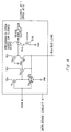
- FIG. 4 shows an embodiment in which device identifying code transistor Q 1E is provided with a data sense circuit 4.
- a sense amplifier comprises transistor T 1 , T 2 , T 3 , T 4 and T 6 .
- the voltage of the bus line B u1 is made low and NMOS transistor T 3 is turned off, thus the NMOS transistors T 4 and T 6 are turned on, thus the current is deprived from a line sense amplifier OUTPUT through NMOS transistor T6, and thus the voltage of the line sense amplifier OUTPUT is made low.
- a signature signal SGH is high, PMOS transistor T 1 is turned off and thus the sense amplifier does not operate.
- the device identifying code is read out from the line sense amplifier OUTPUT of the sense amplifier, depending on whether the switch S 1E provided between the device identifying transistor Q 1E and the line sense amplifier OUTPUT is on or off. That is, when the switch S 1E is opened, the logic “0” is output from sense amplifier OUTPUT and when the switch S 1E is closed, the logic "1" is output.
- Figure 5 shows an embodiment in which a device identifying code circuit element is provided in an output buffer.
- the signature SGH becomes “H” the device identifying code is read out.
- switch A is connected to V ss and switch B is connected to the signal SGH, then output transistor T 19 produces “H” through a NOR circuit comprising transistors T 11 , T 12 , T 13 and T 14 and a NOR circuit comprising transistors T 15 , T 16 , T 17 and T 18 . That is, when switch B is connected to signature SGH and is high, NMOS transistor T 18 is turned on and line L 1 becomes low, enabling the output of output transistor T 19 to be "H".
- the switch A is connected to signature SGH and the switch B is connected to Vss. Therefore, NMOS transistor T 14 becomes conductive and line L 2 becomes low, thereby enabling NMOS transistor T 17 to be nonconductive and PMOS transistor T 16 to be conductive. Therefore, line L 1 becomes high and thus the output of output transistor T 19 becomes "L".
- the signature SGH is low, switch A is connected to Vss and switch B to SGH, both NMOS transistors T 14 and T 18 become nonconductive and thus, the signature SGH for obtaining the device identifying code is cut off from a signal transmission line from sense amplifier OUTPUT, line L 2 , line L 1 , and DATA OUTPUT.
- PMOS transistor T 11 is turned on and when sense amplifier OUTPUT is "H", PMOS transistor T 12 is nonconductive and line L2 is “L”. Then, PMOS transistors T 15 and T 16 become conductive, thereby allowing line L 1 to be "H” and DATA OUTPUT of transistor T 19 to be "L”.
- the output of the sense amplifier is provided at the DATA OUTPUT after the output of the sense amplifier is inverted.
- the output of the data sense circuit is applied to the sense amplifier output line sense amplifier OUTPUT and the device identifying code is read out from the data output through the output transistor T 19 .
- a block comprising a plurality of bit lines can be replaced by a spare block.
- Respective blocks 1 to 4 correspond to the output of the device for producing 4 bit output. If a block 1 is faulty, then signal SP1 turns "H” and SP1 ⁇ turns “L” and then the block 1 corresponding to one output bit of 4 bit output is replaced by a spare block. More specifically, an address signal is applied to blocks 1 to 4 and spare block through row decoder 13 and column decoder 14 and is also applied to a redundant control circuit 15, in which an address corresponding to a faulty cell is stored, for example.
- the embodiments of the RWM as shown in Figures 2 to 6 are designated as being the present invention.
- the RWM circuit structure is not limited to these embodiments as the RWM having other circuit structures is within the scope of the present invention.
- the RWM of the present invention is useful where bit line redundancy does not exist, an RWM which does not have a spare bit line is within the scope of the present invention.
- the device identifying code storing circuit connected to the bus line may be formed of other means for storing the code.
- the circuit structure of the present invention is not limited to the embodiments shown in Figures 2 and 3.
- the other circuit structure may be within the scope of the present invention.
- one cell for storing logic "1" or "0" comprises one transistor, for example Q 1n , but it may comprise a plurality of transistors.
- the device identifying code can be stored in the RWM by programming a program using the device identifying code storing circuit connected to the bus line.
- the device identifying code can be read out without it being affected by a selection of the spare bit line.
Description
- The present invention relates to a programmable semiconductor memory apparatus (called an RWM: Read/Write Memory) and more particularly to an RWM with a circuit for storing a device identifying code.
- An RWM can be generally divided into a RAM (Random Access Memory) and a ROM (Read Only Memory). A programmable ROM corresponds to an RWM. A programmable ROM is classified from the viewpoint of structure into a bipolar-type, a FAMOS (Floating-gate Avalanche Injection MOS) or an MNOS (Metal Nitride Oxide Semiconductor), and classified from the viewpoint of whether it is applied into a fuse ROM (programmable ROM), an EP-ROM(Erasable Programmable ROM), an EEP-ROM (Electrically Erasable and Programmable ROM), or an EA-ROM (Electrically Alterable ROM).
- An RWM is forwarded from the manufacturer in a blank state, i.e., in a state where the data is not written, the user-side writes data by ROM writer. A ROM writer has a function of automatically setting a condition for writing data into an RWM device. Therefore, a circuit for storing a self device identifying code and enabling the self device identifying code to be read upon writing data into RWM is generally provided on the device side. The self device identifying code represents the conditions for writing data into an RWM such as the name of a manufacturer memory capacity, the kind of writing algorithm and chip revision of the RWM.
- Figure 1 shows the structure of a prior art RWM circuit for explaining the operation of the RWM.
- An RWM generally comprises a first
memory cell array 1 to a k-thmemory cell array 3, anddata sense circuits 4. More precisely, a RWM comprises bit lines B1 to Bm, word lines W1 to Wn and Wc, memory transistors Q11 to Qmn, bit line selection transistors Q1s to Qms, device identifying code storing transistors Q1c to Qkc and bus lines Bu1 to Buk. - When a memory write is performed in the RWM, an address signal is produced to select one word line (for example W1) and one bit line (for example B1) to select a predetermined memory transistor Q11, and data is written by applying an "H" signal or an "L" signal to memory transistor circuit Q11. When data is read, a predetermined memory transistor Q11 is selected by the same operation as above, thereby outputting the stored data. Generally, the device identifying code is stored in device identifying code storing transistors Q1c to Qkc connected to the bit line. In the prior art shown in Figure 1, a device identifying code storing transistors Q1c to Qkc is provided for respective memory cell arrays and as k device identifying code storing transistors Q1c to Qkc are used, the number of device identifying codes comprises k bits. In a device of this type, only the exclusive word line Wc may be selected to enable the device identifying code to be read out. This makes a device of this type easy to pattern and thus it is widely used.
- In accordance with a recent increase in the degree of LSI integration, a redundant bit line is generally provided to increase yield. A redundant bit line is provided by preparing several spare bit lines in the memory. Thus, even if a faulty bit line, word line or memory cell exists in a memory, a spare bit line is selected when an address signal selecting the faulty portion enters the memory. Thus, a device containing a fault can be used as if it were fault-free. When a redundant bit line is embodied, there is always a possibility of replacing a discretional bit line by a spare bit line. In this case the replaced bit line is not used thereafter. When the device identifying code storing transistor Qic is connected to the replaced bit line, an element of the device identifying code stored in the device identifying code storing transistor Qic, for example, the i-th element of the k-bit code, is lacking and thus cannot be read out. This prevents the device identifying code from performing an effective function. Therefore, when the bit line redundancy is embodied, the type with the device identifying code stored in the device identifying code storing transistor connected to the bit line cannot be used.
- From Patent Abstracts of Japan, vol. 8, no. 282 (P-323), Dec. 1984, & JP-A-59 146 498, a semiconductor memory having bit lines, spare bit lines and a bus line as described in the preamble of
claim 1 is known. - Document US-A-4,055,802 discloses a configuration with the purpose to provide a technology by which a circuit configuration can be electrically identified. A cathode of a diode is connected to respective input lines (or output lines) of a chip in a ROM and an electrical switch is provided at an anode side of the diode for switching over the coupling to ground or an emitter of the transistor. When an electrical interrogation signal is applied to the input lines an unique pattern appears representative of the particular circuit. Thus, from this document, a semiconductor memory is known having identifying code storing means connected to input lines or output lines.
- An object of the present invention is to provide an improved RWM capable of storing the device identifying code to enable the device identifying code to be easily read out even when a bit line redundancy is adopted.
- According to the invention, this object is achieved by a programmable semiconductor memory apparatus according to
claim 1. -
- Figure 1 shows a circuit diagram of an example of a conventional RWM,
- Figure 2 shows a circuit diagram of a first embodiment of the RWM of the present invention,
- Figure 3 shows a circuit diagram of a second embodiment of the RWM of the present invention,
- Figure 4 shows another embodiment of the present invention,
- Figure 5 shows a further embodiment of the present invention, and
- Figure 6 shows a still further embodiment of the present invention.
- An embodiment of the present invention will be explained by referring to the drawings.
- Figure 2 shows the first embodiment of the present invention. In Figure 2, the same parts as those in the prior art shown in Figure 1 are provided with the same reference numbers, and detailed explanations of such parts are omitted.
- A programmable semiconductor memory apparatus comprises
memory cell arrays data sense circuits 4 for writing data into and reading data from saidmemory cell arrays memory cell arrays - In the present invention with the above structure, even when a bit line redundancy is embodied in an RWM, a discretional spare bit line is selected in place of a faulty bit line. The device identifying code is not stored in device identifying code storing transistors Q1c to Qkc connected to the bit line as in the case of the prior art RWM, but in a memory circuit connected to bus lines Bu1 to Buk provided between the common node of the bit lines B1 to Bm and Bs1 to Bsj and the
data sense circuits 4. Therefore, even if one of the faulty bit lines is disposed of, and instead any spare bit line is selected, a device identifying code can be correctly read out without being affected. - In Figure 2, the portions which are different from those in Figure 1 are as follows. Spare bit lines Bs1 to Bsj are provided, the device identifying code storing transistors Q1c to Qkc connected to the bit lines B1 to Bm are deleted and instead the device identifying code storing transistors Q1D to QkD connected to bus lines Bu1 to Buk are newly provided. The number of spare bit lines is not limited to 1 per respective memory cell array. Gss to Gsj represent gate terminals of spare bit line selecting transistors Qss to Qsj. When the address signal for selecting a faulty bit line, for example B2, enters gate G2s, an "H" signal for selecting a spare bit line, for example Bs1, is applied to gate Gss and bit line B2 is replaced by spare bit line Bs1.
- A device identifying code is programmed in device identifying code storing transistors Q1D to QkD upon the manufacturing of an RWM.
- Device identifying code storing transistors Q1D to QkD are turned on when an (H) signal more than threshold voltage VTH is applied to the gates G1D to GkD thereof and they are turned off when an (L) signal less than the threshold voltage VTH is applied to G1D to GkD thereof. Thus, the device identifying storing transistors Q1D to QkD are of the enhancement type. Device identifying code storing transistors Q1D to QkD are of the type having a threshold voltage VTH changed by an electric operation. For example, the transistors Q1D to QkD are formed such that in accordance with an electrical operation, they have two threshold voltages comprising a voltage V1 which is higher than the source voltage Vcc and a voltage V2 which is lower than the source voltage Vcc. Codes determined as being logic "0" or "1" depending on voltages V1 and V2 are provided for respective device identifying code storing transistors Q1D to QkD. When the power source voltage Vcc is applied to gates G1D to GkD, the transistor with the threshold voltage of V1 is turned off and the transistor with the threshold voltage V2 is turned on. Namely, k bits of device identifying code can be stored by determining that logic "0" corresponds to voltage V1 and logic "1" corresponds to voltage V2, depending on whether the threshold voltage of the transistors Q1D to QkD is determined as being V1 or V2. Conversely, k bits of device identifying code may be stored by determining that logic "1" corresponds to voltage V1 and logic "0" corresponds to voltage V2. In other words, the device identifying code can be programmed based on threshold voltages V1 and V2 of device identifying storing transistors Q1D to QkD.
- Address signals ADo to ADn and signature signal

NAND circuit 11. The output ofNAND circuit 11 is applied to gates G1s to Gms of bit line selecting transistors Q1s to Qms and gates Gss to Gsj of spare bit line selecting transistors Qss to Qsj throughinverter 12. - Next, the operation of the present invention will be explained.
- When a memory write and memory read is performed, the same operation as in the ordinary RWM is conducted and one memory transistor, for example, Q11, is selected and the data to be stored is input to the RWM.
- When the device identifying code is read out, an "L" signal is applied to all the gates of G1s to Gms of bit line selecting transistors Q1s to Qms and gates Gss to Gsj of spare bit line selecting transistors Qss to Qsj from
inverter 12, as signature singal SGH is turned high. Thus all the bit lines are electrically disconnected from the bus lines Bu1 to Buk. Next, source voltage Vcc is applied to gates G1D to GkD of device identifying code storing transistors Q1D to QkD and thus the device identifying code can be read out. Alternatively, NMOS transistors may be provided between the common nodes of bit lines and a spare bit line formingmemory cell arrays 
- Figure 3 shows the second embodiment of the present invention. This embodiment is different from that in Figure 2 in that device identifying storing transistors Q1E to QkE are provided in place of device identifying code storing transistors Q1D to QkD shown in Figure 2, and electric switching means S1E to SkE are provided on a line connecting device identifying code storing transistors Q1E to QkE and bus lines Bu1 to Buk.
- Device identifying code storing transistor Q1E to QkE are different from device identifying code storing transistors Q1D to QkD in that the threshold voltage VTH may not be variable in accordance with an electric operation. Transistors Q1D to QkD turn on when an (H) signal is applied to gates G1E to GkE. In the second embodiment the threshold voltage VTH is made less than or equal to power source voltage Vcc.
- In the second embodiment, the device identifying code is programmed by using electric switching means S1E to SkE. Electric switching means S1E to SkE may be of the so-called fuse type which are conductive before programming but are melted to be cut out or made nonconductive by an application of a current upon programming. Electric switching means S1E to SkE may also be of the type which are nonconductive before programming but, are made conductive by an application of a current upon programming when connected through melting. It is possible to program the device identifying code by determining logic "1" for ON and determining logic "0" for OFF, depending on whether the electric switching means is conductive (ON) or nonconductive (OFF). Conversely, the program of the device identifying code may be performed so that logic "1" is determined for OFF and logic "0" for ON for electric switching means S1E to SkE. In this case, the device identifying code comprises k-bit code, as the number of the electric switching means is k.
- Next, the operation will be explained. In case of a memory write or read, the same operation as in the first embodiment may be performed.
- When the device identifying code is read, an (L) signal is applied to all the gates of bit line selection transistors Q1S to Qms and gates Gss to Gsj of spare bit line selection transistors Qss to Qsj and all the bit lines are cut off from bus lines Bu1 to Buk. Next, when the source voltage Vcc is applied to gate G1E to GkE of device identifying code storing transistors Q1E to QkE, the device identifying code is programmed depending on the on-and-off electric switching means S1E to SkE.
- Figure 4 shows an embodiment in which device identifying code transistor Q1E is provided with a
data sense circuit 4. A sense amplifier comprises transistor T1, T2, T3, T4 and T6. When the data is not stored in a cell connected to the bus line Bu1, the voltage of the bus line Bu1 is made low and NMOS transistor T3 is turned off, thus the NMOS transistors T4 and T6 are turned on, thus the current is deprived from a line sense amplifier OUTPUT through NMOS transistor T6, and thus the voltage of the line sense amplifier OUTPUT is made low. As a result, low data is read from the cell. When a signature signal SGH is high, PMOS transistor T1 is turned off and thus the sense amplifier does not operate. When the signature signal SGH applied to the device identifying code NMOS transistor Q1E is high, the device identifying code is read out from the line sense amplifier OUTPUT of the sense amplifier, depending on whether the switch S1E provided between the device identifying transistor Q1E and the line sense amplifier OUTPUT is on or off. That is, when the switch S1E is opened, the logic "0" is output from sense amplifier OUTPUT and when the switch S1E is closed, the logic "1" is output. In this embodiment, when the device identifying code is read out, it is necessary both to apply an "L" signal to all the gates of the bit line selection transistors and spare bit line selection transistors and to apply a high signature signal SGH "H" to the gate of the device identifying NMOS transistor Q1E. - Figure 5 shows an embodiment in which a device identifying code circuit element is provided in an output buffer. When the signature SGH becomes "H" the device identifying code is read out. When switch A is connected to Vss and switch B is connected to the signal SGH, then output transistor T19 produces "H" through a NOR circuit comprising transistors T11, T12, T13 and T14 and a NOR circuit comprising transistors T15, T16, T17 and T18. That is, when switch B is connected to signature SGH and is high, NMOS transistor T18 is turned on and line L1 becomes low, enabling the output of output transistor T19 to be "H". Next, in order to make the data output "L", the switch A is connected to signature SGH and the switch B is connected to Vss. Therefore, NMOS transistor T14 becomes conductive and line L2 becomes low, thereby enabling NMOS transistor T17 to be nonconductive and PMOS transistor T16 to be conductive. Therefore, line L1 becomes high and thus the output of output transistor T19 becomes "L". When the signature SGH is low, switch A is connected to Vss and switch B to SGH, both NMOS transistors T14 and T18 become nonconductive and thus, the signature SGH for obtaining the device identifying code is cut off from a signal transmission line from sense amplifier OUTPUT, line L2, line L1, and DATA OUTPUT. In this case, PMOS transistor T11 is turned on and when sense amplifier OUTPUT is "H", PMOS transistor T12 is nonconductive and line L2 is "L". Then, PMOS transistors T15 and T16 become conductive, thereby allowing line L1 to be "H" and DATA OUTPUT of transistor T19 to be "L". Thus, when the signature SGH is "L", the output of the sense amplifier is provided at the DATA OUTPUT after the output of the sense amplifier is inverted. In this embodiment the output of the data sense circuit is applied to the sense amplifier output line sense amplifier OUTPUT and the device identifying code is read out from the data output through the output transistor T19.
- As shown in Figure 6, instead of replacing a faulty bit line by a spare bit line, a block comprising a plurality of bit lines can be replaced by a spare block.
Respective blocks 1 to 4 correspond to the output of the device for producing 4 bit output. If ablock 1 is faulty, then signal SP1 turns "H" and
block 1 corresponding to one output bit of 4 bit output is replaced by a spare block. More specifically, an address signal is applied toblocks 1 to 4 and spare block throughrow decoder 13 andcolumn decoder 14 and is also applied to aredundant control circuit 15, in which an address corresponding to a faulty cell is stored, for example. Thus, when the address signal corresponding to the faulty cell is applied toredundant control circuit 15,switch 16 is turned to Vcc . Thus, SPn becomes high and
inverter 17, thereby selecting the spare block. Device identifying code storing transistors are respectively connected toblocks 1 to 4 and spare block through electric switching means and bus lines in the same manner as shown in Figure 2 and 3. Data D1 to D4 are read out from the data sense circuit. Therefore, the present invention can be applied to the embodiment shown in Figure 6 in which the faulty bit line block among therespective blocks 1 to 4 can be replaced by a spare block. The present invention is also applicable to the case where each ofrespective blocks 1 to 4 comprise one bit line. - The embodiments of the RWM as shown in Figures 2 to 6 are designated as being the present invention. However, the RWM circuit structure is not limited to these embodiments as the RWM having other circuit structures is within the scope of the present invention. For example, as the RWM of the present invention is useful where bit line redundancy does not exist, an RWM which does not have a spare bit line is within the scope of the present invention. The device identifying code storing circuit connected to the bus line may be formed of other means for storing the code. The circuit structure of the present invention is not limited to the embodiments shown in Figures 2 and 3. The other circuit structure may be within the scope of the present invention. In the above embodiments, one cell for storing logic "1" or "0" comprises one transistor, for example Q1n, but it may comprise a plurality of transistors.
- As described above, according to the present invention, even if bit line redundancy exists in the RWM, the device identifying code can be stored in the RWM by programming a program using the device identifying code storing circuit connected to the bus line. Thus, even if the fault bit line is disposed and the spare bit line is selected, the device identifying code can be read out without it being affected by a selection of the spare bit line.
Claims (8)
- A programmable semiconductor memory apparatus in which bit line redundancy is adopted comprising:a memory cell array (1, 2, 3);a plurality of bit lines (B1, B2, ...) connected to said memory cell array;at least one spare bit line (BS1, BS2, ...) which is switched and used if said plurality of bit lines (B1, B2, ...) includes faulty bit lines;at least a bus line (Bu1, Bu2, ...) connected to one of said bit lines (B1, B2, ... ) or said at least one spare bit line (Bs1, Bs2, ...) in response to an address signal (Gms, Gsj) ;a data sense circuit (4) connected to said at least one bus line for reading data from said memory cell array,characterized byat least a storing means (Q1E, Q2E, ...) for storing an identifying code for identifying said programmable semiconductor memory apparatus, said storing means being coupled to the output of the data sense circuit (4), thereby enabling said identifying code to be read externally without lack of bits of said identifying code if faulty bit lines (B1, B2, ...) are replaced by spare bit lines (Bs1, Bs2, ...);a switch means (T1, T2) connected to said data sense circuit (4), for receiving a signature signal (SGH) designating that the identifying code has been read out from said storing means (Q1E, Q2E, ...) and for producing the identifying code regardless of the input of the data sense circuit (4), said switch means (T1, T2) affecting said data sense circuit (4) such that the identifying code appears at the output of said data sense circuit (4).
- The programmable semiconductor memory apparatus according to claim 1,
characterized in that
all word lines (W1, W2, ...) of said memory cell array (1, 2, 3) are made non-active when the identifying code is read out. - The programmable semiconductor memory apparatus according to claim 1 or 2,
characterized in thatsaid storing means comprises a transistor having a first threshold voltage or a second threshold voltage; andthe transistor becomes conductive or non-conductive when a gate voltage is applied to said transistor, thereby providing logic "1" and "0", respectively. - The programmable semiconductor memory apparatus according to claim 1 or 2,
characterized in that
said storing means comprises a transistor (Q1E, Q2E, ...) connected to the bus line (Bu1, Bu2, ...) through a fuse (S1E, S2E, ...) provided between the drain and the bus line (Bu1, Bu2, ...). - The programmable semiconductor memory apparatus according to anyone of claims 1 - 4,
characterized in that
said storing means is provided within said data sense circuit (4). - The programmable semiconductor memory apparatus according to anyone of the claims 1 - 4,
characterized in that
said storing means is provided within an output buffer circuit. - The programmable semiconductor memory apparatus according to anyone of claims 1 to 6,
characterized in that
said switching means controls a gate of a pull-up transistor to determine whether a data from said data sense circuit (4) is output or said identifying code is output. - The programmable semiconductor memory apparatus according to anyone of the claims 1 to 4,
characterized in thatsaid memory cell array (1, 2, 3) is divided into respective blocks connected to bit lines and spare blocks connected to spare bit lines, one of said bit lines and one of said spare bit lines of each block being connected to one of said bus lines, each one of said bus lines being connected to one of said storing means; andswitching means are provided between said respective block and said bus line and between said spare block and said bus line, and switch and connect said spare block to said bus line in place of said respective blocks when said respective blocks are faulty.
Applications Claiming Priority (2)
| Application Number | Priority Date | Filing Date | Title |
|---|---|---|---|
| JP17830489A JP2582439B2 (en) | 1989-07-11 | 1989-07-11 | Writable semiconductor memory device |
| JP178304/89 | 1989-07-11 |
Publications (3)
| Publication Number | Publication Date |
|---|---|
| EP0408002A2 EP0408002A2 (en) | 1991-01-16 |
| EP0408002A3 EP0408002A3 (en) | 1992-06-03 |
| EP0408002B1 true EP0408002B1 (en) | 1996-10-30 |
Family
ID=16046133
Family Applications (1)
| Application Number | Title | Priority Date | Filing Date |
|---|---|---|---|
| EP90113258A Expired - Lifetime EP0408002B1 (en) | 1989-07-11 | 1990-07-11 | A programmable semiconductor memory apparatus |
Country Status (5)
| Country | Link |
|---|---|
| US (1) | US4998223A (en) |
| EP (1) | EP0408002B1 (en) |
| JP (1) | JP2582439B2 (en) |
| KR (1) | KR930009542B1 (en) |
| DE (1) | DE69029013T2 (en) |
Families Citing this family (24)
| Publication number | Priority date | Publication date | Assignee | Title |
|---|---|---|---|---|
| US5680353A (en) * | 1988-09-14 | 1997-10-21 | Sgs-Thomson Microelectronics, S.A. | EPROM memory with internal signature concerning, in particular, the programming mode |
| JP2547633B2 (en) * | 1989-05-09 | 1996-10-23 | 三菱電機株式会社 | Semiconductor memory device |
| US5289417A (en) * | 1989-05-09 | 1994-02-22 | Mitsubishi Denki Kabushiki Kaisha | Semiconductor memory device with redundancy circuit |
| US5343406A (en) * | 1989-07-28 | 1994-08-30 | Xilinx, Inc. | Distributed memory architecture for a configurable logic array and method for using distributed memory |
| JPH03241598A (en) * | 1990-02-19 | 1991-10-28 | Fujitsu Ltd | Signature circuit |
| JPH043399A (en) * | 1990-04-19 | 1992-01-08 | Sharp Corp | Semiconductor memory |
| US5204841A (en) * | 1990-07-27 | 1993-04-20 | International Business Machines Corporation | Virtual multi-port RAM |
| US5793667A (en) * | 1990-09-19 | 1998-08-11 | The United States Of America As Represented By The Secretary Of The Navy | Sense amplifier control system for ferroelectric memories |
| JPH04132089A (en) * | 1990-09-20 | 1992-05-06 | Nec Ic Microcomput Syst Ltd | Eprom with built-in identification code |
| JP2724046B2 (en) * | 1991-02-07 | 1998-03-09 | 富士写真フイルム株式会社 | IC memory card system |
| US5197029A (en) * | 1991-02-07 | 1993-03-23 | Texas Instruments Incorporated | Common-line connection for integrated memory array |
| JP3128362B2 (en) * | 1992-12-04 | 2001-01-29 | 富士通株式会社 | Semiconductor device |
| JPH0785685A (en) * | 1993-09-17 | 1995-03-31 | Fujitsu Ltd | Semiconductor device |
| JPH07272499A (en) * | 1994-03-30 | 1995-10-20 | Mitsubishi Electric Corp | Semiconductor memory device |
| US5499211A (en) * | 1995-03-13 | 1996-03-12 | International Business Machines Corporation | Bit-line precharge current limiter for CMOS dynamic memories |
| JP3531891B2 (en) * | 1996-01-26 | 2004-05-31 | シャープ株式会社 | Semiconductor storage device |
| US6188239B1 (en) * | 1996-08-12 | 2001-02-13 | Micron Technology, Inc. | Semiconductor programmable test arrangement such as an antifuse to ID circuit having common access switches and/or common programming switches |
| US5976917A (en) | 1998-01-29 | 1999-11-02 | Micron Technology, Inc. | Integrated circuitry fuse forming methods, integrated circuitry programming methods, and related integrated circuitry |
| US6609169B1 (en) | 1999-06-14 | 2003-08-19 | Jay Powell | Solid-state audio-video playback system |
| JP4645837B2 (en) * | 2005-10-31 | 2011-03-09 | 日本電気株式会社 | Memory dump method, computer system, and program |
| JP4745072B2 (en) * | 2006-02-02 | 2011-08-10 | 日本無線株式会社 | Receiver |
| JP4704229B2 (en) * | 2006-02-02 | 2011-06-15 | 日本無線株式会社 | Receiver |
| US20110099423A1 (en) * | 2009-10-27 | 2011-04-28 | Chih-Ang Chen | Unified Boot Code with Signature |
| KR102532528B1 (en) * | 2016-04-07 | 2023-05-17 | 에스케이하이닉스 주식회사 | Memory device and operating method thereof |
Citations (1)
| Publication number | Priority date | Publication date | Assignee | Title |
|---|---|---|---|---|
| EP0239021A2 (en) * | 1986-03-20 | 1987-09-30 | Fujitsu Limited | Semiconductor memory device |
Family Cites Families (11)
| Publication number | Priority date | Publication date | Assignee | Title |
|---|---|---|---|---|
| US4055802A (en) * | 1976-08-12 | 1977-10-25 | Bell Telephone Laboratories, Incorporated | Electrical identification of multiply configurable circuit array |
| CA1158775A (en) * | 1980-06-04 | 1983-12-13 | Thomas L. Phinney | Computer annotation system |
| JPS59146498A (en) * | 1983-02-10 | 1984-08-22 | Fujitsu Ltd | Semiconductor memory |
| US4622653A (en) * | 1984-10-29 | 1986-11-11 | Texas Instruments Incorporated | Block associative memory |
| US4667313A (en) * | 1985-01-22 | 1987-05-19 | Texas Instruments Incorporated | Serially accessed semiconductor memory with tapped shift register |
| US4744062A (en) * | 1985-04-23 | 1988-05-10 | Hitachi, Ltd. | Semiconductor integrated circuit with nonvolatile memory |
| JPS61258399A (en) * | 1985-05-11 | 1986-11-15 | Fujitsu Ltd | Semiconductor integrated circuit device |
| JPS62217498A (en) * | 1986-03-06 | 1987-09-24 | Fujitsu Ltd | Semiconductor memory device |
| US4789967A (en) * | 1986-09-16 | 1988-12-06 | Advanced Micro Devices, Inc. | Random access memory device with block reset |
| JPH0632213B2 (en) * | 1987-02-26 | 1994-04-27 | 日本電気株式会社 | Semiconductor memory |
| JPH01109599A (en) * | 1987-10-22 | 1989-04-26 | Nec Corp | Writable and erasable semiconductor memory device |
-
1989
- 1989-07-11 JP JP17830489A patent/JP2582439B2/en not_active Expired - Lifetime
-
1990
- 1990-07-10 US US07/550,786 patent/US4998223A/en not_active Expired - Lifetime
- 1990-07-11 KR KR1019900010466A patent/KR930009542B1/en not_active IP Right Cessation
- 1990-07-11 EP EP90113258A patent/EP0408002B1/en not_active Expired - Lifetime
- 1990-07-11 DE DE69029013T patent/DE69029013T2/en not_active Expired - Lifetime
Patent Citations (1)
| Publication number | Priority date | Publication date | Assignee | Title |
|---|---|---|---|---|
| EP0239021A2 (en) * | 1986-03-20 | 1987-09-30 | Fujitsu Limited | Semiconductor memory device |
Also Published As
| Publication number | Publication date |
|---|---|
| DE69029013D1 (en) | 1996-12-05 |
| DE69029013T2 (en) | 1997-05-28 |
| EP0408002A3 (en) | 1992-06-03 |
| EP0408002A2 (en) | 1991-01-16 |
| JPH0344899A (en) | 1991-02-26 |
| KR930009542B1 (en) | 1993-10-06 |
| JP2582439B2 (en) | 1997-02-19 |
| KR910003677A (en) | 1991-02-28 |
| US4998223A (en) | 1991-03-05 |
Similar Documents
| Publication | Publication Date | Title |
|---|---|---|
| EP0408002B1 (en) | A programmable semiconductor memory apparatus | |
| US4514830A (en) | Defect-remediable semiconductor integrated circuit memory and spare substitution method in the same | |
| US4603404A (en) | Semiconductor memory device with redundant cells | |
| US5003205A (en) | Buffer circuit used in a semiconductor device operating by different supply potentials and method of operating the same | |
| US6700821B2 (en) | Programmable mosfet technology and programmable address decode and correction | |
| EP0110636B1 (en) | Improvements in or relating to semiconductor memories | |
| US5485424A (en) | Semiconductor memory and redundant-address writing method | |
| US6650567B1 (en) | Nonvolatile semiconductor memories with a NAND logic cell structure | |
| EP0085386A2 (en) | Semiconductor device with spare memory cells | |
| JPH0528787A (en) | Redundancy circuit for nonvolatile semiconductor memory | |
| US5434814A (en) | Circuit for repairing defective read only memories with redundant NAND string | |
| US4794568A (en) | Redundancy circuit for use in a semiconductor memory device | |
| EP0131930B1 (en) | Semiconductor memory device | |
| US4656609A (en) | Semiconductor memory device | |
| US6198659B1 (en) | Defective address data storage circuit for nonvolatile semiconductor memory device having redundant function and method of writing defective address data | |
| US4571706A (en) | Semiconductor memory device | |
| US5644529A (en) | Integrated circuit for the programming of a memory cell in a non-volatile memory register | |
| US5696716A (en) | Programmable memory element | |
| US20080062738A1 (en) | Storage element and method for operating a storage element | |
| JPS59151400A (en) | Semiconductor storage device | |
| US5319599A (en) | Redundancy circuit for semiconductor memory device | |
| EP0377841A2 (en) | Semiconductor integrated circuit capable of preventing occurrence of erroneous operation due to noise | |
| US6249478B1 (en) | Address input circuit and semiconductor memory using the same | |
| EP0427260B1 (en) | Non-volatile memory devices | |
| JPH0219560B2 (en) |
Legal Events
| Date | Code | Title | Description |
|---|---|---|---|
| PUAI | Public reference made under article 153(3) epc to a published international application that has entered the european phase |
Free format text: ORIGINAL CODE: 0009012 |
|
| AK | Designated contracting states |
Kind code of ref document: A2 Designated state(s): DE FR GB |
|
| PUAL | Search report despatched |
Free format text: ORIGINAL CODE: 0009013 |
|
| AK | Designated contracting states |
Kind code of ref document: A3 Designated state(s): DE FR GB |
|
| 17P | Request for examination filed |
Effective date: 19920629 |
|
| 17Q | First examination report despatched |
Effective date: 19931228 |
|
| GRAG | Despatch of communication of intention to grant |
Free format text: ORIGINAL CODE: EPIDOS AGRA |
|
| GRAH | Despatch of communication of intention to grant a patent |
Free format text: ORIGINAL CODE: EPIDOS IGRA |
|
| GRAH | Despatch of communication of intention to grant a patent |
Free format text: ORIGINAL CODE: EPIDOS IGRA |
|
| GRAA | (expected) grant |
Free format text: ORIGINAL CODE: 0009210 |
|
| AK | Designated contracting states |
Kind code of ref document: B1 Designated state(s): DE FR GB |
|
| REF | Corresponds to: |
Ref document number: 69029013 Country of ref document: DE Date of ref document: 19961205 |
|
| ET | Fr: translation filed | ||
| PLBE | No opposition filed within time limit |
Free format text: ORIGINAL CODE: 0009261 |
|
| STAA | Information on the status of an ep patent application or granted ep patent |
Free format text: STATUS: NO OPPOSITION FILED WITHIN TIME LIMIT |
|
| 26N | No opposition filed | ||
| REG | Reference to a national code |
Ref country code: GB Ref legal event code: IF02 |
|
| REG | Reference to a national code |
Ref country code: GB Ref legal event code: 732E |
|
| REG | Reference to a national code |
Ref country code: FR Ref legal event code: TP |
|
| PGFP | Annual fee paid to national office [announced via postgrant information from national office to epo] |
Ref country code: FR Payment date: 20090710 Year of fee payment: 20 |
|
| PGFP | Annual fee paid to national office [announced via postgrant information from national office to epo] |
Ref country code: GB Payment date: 20090708 Year of fee payment: 20 Ref country code: DE Payment date: 20090709 Year of fee payment: 20 |
|
| REG | Reference to a national code |
Ref country code: GB Ref legal event code: PE20 Expiry date: 20100710 |
|
| REG | Reference to a national code |
Ref country code: FR Ref legal event code: CD Ref country code: FR Ref legal event code: CA |
|
| PG25 | Lapsed in a contracting state [announced via postgrant information from national office to epo] |
Ref country code: GB Free format text: LAPSE BECAUSE OF EXPIRATION OF PROTECTION Effective date: 20100710 |
|
| PG25 | Lapsed in a contracting state [announced via postgrant information from national office to epo] |
Ref country code: DE Free format text: LAPSE BECAUSE OF EXPIRATION OF PROTECTION Effective date: 20100711 |