EP0496391A2 - Semiconductor memory device - Google Patents
Semiconductor memory device Download PDFInfo
- Publication number
- EP0496391A2 EP0496391A2 EP92101072A EP92101072A EP0496391A2 EP 0496391 A2 EP0496391 A2 EP 0496391A2 EP 92101072 A EP92101072 A EP 92101072A EP 92101072 A EP92101072 A EP 92101072A EP 0496391 A2 EP0496391 A2 EP 0496391A2
- Authority
- EP
- European Patent Office
- Prior art keywords
- address pointer
- data
- mode
- serial
- port
- Prior art date
- Legal status (The legal status is an assumption and is not a legal conclusion. Google has not performed a legal analysis and makes no representation as to the accuracy of the status listed.)
- Granted
Links
Images

Classifications
-
- G—PHYSICS
- G11—INFORMATION STORAGE
- G11C—STATIC STORES
- G11C11/00—Digital stores characterised by the use of particular electric or magnetic storage elements; Storage elements therefor
- G11C11/21—Digital stores characterised by the use of particular electric or magnetic storage elements; Storage elements therefor using electric elements
- G11C11/34—Digital stores characterised by the use of particular electric or magnetic storage elements; Storage elements therefor using electric elements using semiconductor devices
- G11C11/40—Digital stores characterised by the use of particular electric or magnetic storage elements; Storage elements therefor using electric elements using semiconductor devices using transistors
-
- G—PHYSICS
- G11—INFORMATION STORAGE
- G11C—STATIC STORES
- G11C29/00—Checking stores for correct operation ; Subsequent repair; Testing stores during standby or offline operation
- G11C29/04—Detection or location of defective memory elements, e.g. cell constructio details, timing of test signals
- G11C29/08—Functional testing, e.g. testing during refresh, power-on self testing [POST] or distributed testing
- G11C29/12—Built-in arrangements for testing, e.g. built-in self testing [BIST] or interconnection details
- G11C29/18—Address generation devices; Devices for accessing memories, e.g. details of addressing circuits
- G11C29/20—Address generation devices; Devices for accessing memories, e.g. details of addressing circuits using counters or linear-feedback shift registers [LFSR]
-
- G—PHYSICS
- G11—INFORMATION STORAGE
- G11C—STATIC STORES
- G11C29/00—Checking stores for correct operation ; Subsequent repair; Testing stores during standby or offline operation
- G11C29/02—Detection or location of defective auxiliary circuits, e.g. defective refresh counters
-
- G—PHYSICS
- G11—INFORMATION STORAGE
- G11C—STATIC STORES
- G11C7/00—Arrangements for writing information into, or reading information out from, a digital store
- G11C7/10—Input/output [I/O] data interface arrangements, e.g. I/O data control circuits, I/O data buffers
- G11C7/1075—Input/output [I/O] data interface arrangements, e.g. I/O data control circuits, I/O data buffers for multiport memories each having random access ports and serial ports, e.g. video RAM
Definitions
- the present invention relates to a semiconductor memory device, and more particularly to a multi-port semiconductor memory device having a RAM port for randomly accessing memory cells and a SAM port for serially accessing memory cells.
- a multi-port semiconductor memory device having a RAM port for randomly accessing memory cells and a SAM port for serially accessing data in units of the row.
- This device has a register for storing one row data for serial access and means for data transfer between the register and memory cells.
- the RAM port operates asynchronously with the SAM port.
- the data transferring means transfers data between the register and memory cells, stopping the operation of the SAM port.
- an address pointer to the start address for read/write of the SAM port is obtained at the timing when a row address signal is received.
- the SAM port selects the register using a serial counter in the memory device. Therefore, if data outputted from the SAM port is erroneous, it is difficult to discriminate between a fault in obtaining the address pointer and a fault in the data itself.
- the present invention provides a semiconductor memory device of a multi-port structure having a RAM port for randomly accessing a memory cell array having memory cells disposed in matrix and a SAM port for serially accessing data of one row of the array, comprising mode switching means for switching the operation mode of the SAM port between an ordinary data output mode and a test mode, upon externally receiving a mode switching signal; and address pointer outputting means for outputting an address pointer of the SAM port when the operation mode is switched to the test mode by said mode switching means.
- the address pointer outputting means includes an output buffer circuit which in the same output buffer circuit for outputting data from the SAM port, the same output buffer circuit is used in common for both purposes, reducing the size of the memory device.
- the output buffer circuit is used in common and the bit configuration of the SAM port is smaller than the number of bits of the address pointer, the number of output terminals is insufficient for outputting the address pointer at a time.
- the address pointer can be monitored indirectly by outputting the logical sum of at least two parts obtained by dividing the address pointer.
- Fig. 1 is a circuit diagram showing the structure of a semiconductor memory device according to an embodiment of the present invention.
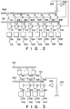
- Fig. 2 is a circuit diagram showing the structure of a circuit portion of the device shown in Fig. 1 for executing a mode change.
- Fig. 3 is a circuit diagram showing another structure of the circuit portion of the device shown in Fig. 1 for executing the mode change.
- FIG. 1 shows the structure of a semiconductor memory device of the embodiment.
- a RAM port Provided as a RAM port is a memory cell array 1 having memory cells of M rows ⁇ N columns ⁇ L bits.
- a row decoder 2 and column decoder 3 are provided. Random access is executed using the accessing means in the following manner.
- a central processing unit (CPU) not shown in Fig. 1 outputs a row address signal and a column address signal.
- the row address signal is amplified by a row address buffer 100 and decoded by the row decoder 2 to select one of the rows.
- the column address signal is amplified by a column address buffer 101 and decoded by the column decoder 3 to open the column select gate 8 of one of the columns. In this manner, one particular row and one particular column are selected to thereby access one memory cell.
- the data applied to a RAM port output pad 202 is supplied to a data buffer 105 via a data input buffer 106 and written in the memory cell via a column line selected by the column select gate.
- the data sensed from the cell is outputted via the data buffer 105, data output buffer 107 and RAM port output pad 202, to an external circuit.
- a data register 4 of N ⁇ L bits and a data transfer gate used for transfer data from the memory cell array 1 to the data register 4.
- a serial accessing means for N data are provided as a serial counter 102, serial decoder 6 and serial select gate 7.
- the serial counter 102 is supplied with an output of the column address buffer 101 during the preceding data transfer cycle, the address pointer being initialized beforehand.
- a serial control signal SC externally inputted to the input terminal 200 of a control circuit 109 rises, the count of the serial counter 102 is incremented by 1, incrementing the address pointer by 1.
- This address pointer is supplied to the serial decoder 6 to decode it.
- the decoded address pointer is outputted to the serial select gate 7.
- the data register corresponding to the decoded address pointer is connected to a serial digit line extending in the lateral direction within the serial select gates 7.
- the data registers starting from the lower bit are sequentially connected to the serial digit line by the serial select gates 7.
- data stored in the data registers 4 is serially outputted from the serial select gates 7.
- the data is then amplified by a aerial data buffer 103, and outputted via a serial output buffer 104 and SAM output port pad 201 to an external circuit.
- the data read during the preceding cycle is outputted from the serial data output buffer 104 to the external circuit.
- Data transfer between the RAM port and SAM port is carried out using a data transfer gate 5.
- the data transfer gate 5 opens to allow the data to be transferred between memory cells of a selected row in the array 1 and the data register 4.
- the serial data output buffer 104 is connected to the serial data line 500 to output the data read from the data register during the preceding cycle.
- the operation mode is switched to a test mode.
- the serial data output buffer 104 is connected to the serial address pointer line 501 so output the address pointer from the serial counter 102.
- Fig. 2 shows the structure of a circuit for switching the serial data output buffer 104 from the serial data line 500 to the serial address pointer line 501 upon input of a signal to the test mode select pad 203.
- serial data line 500 Connected to the serial data line 500 are the drains of N-channel MOS transistors 301 to 308 the sources of which are connected to serial data output buffers 321 to 328. Each gate is connected via an inverter 300 to the test mode select pad 203.
- serial address pointer line 501 Connected to the serial address pointer line 501 are the drains of N-channel MOS transistors 311 to 318, the gates of which are connected to the test mode select pad 203, and the sources of which are connected to the serial data output buffers 321 to 328.
- the serial data output buffers 321 to 328 are provided with SAM port output pads 331 to 338, respectively.
- a low level signal is applied to the test mode select pad 203 and to the gates of the N-channel MOS transistors 311 to 318 to turn them off, so that the serial address pointer line 501 is electrically isolated from the serial data output buffers 321 to 328.
- a high level signal inverted by the inverter 300 is applied to the gates of the N-channel MOS transistors 301 to 308, so that the serial data line 500 is connected to the serial data output buffers 321 to 328. In this manner, data read from the data register 4 is outputted from the SAM port output pads 331 to 338.
- test mode a signal of a power supply potential is applied to the test mode select pad 203, so that the N-channel MOS transistors 311 to 318 turn on to connect the serial address pointer line 501 to the serial data output buffers 321 to 328. Therefore, the N-channel MOS transistors 301 to 308 turn off to disconnect the serial data line 500 from the serial data output buffers 321 to 328. As a result, an address pointer is outputted from the SAM port output pads 331 to 338.
- the circuit structure shown in Fig. 2 corresponds to the case wherein the number of bits of the address pointer is eight bits, the same as that of the SAM port bit configuration. Therefore, the eight bits of the address pointer can be outputted at a time from the eight serial data output buffers 321 to 328.
- the address pointer cannot be outputted at a time from the serial data output buffers.
- the SAM port bit configuration is four bits, and the address pointer is nine bits.
- the address pointer is divided into three parts each having three bits. A logical sum of respective three bits is outputted to each of four serial data output buffers.
- serial address pointer line 501 is connected to the input terminals of three-input AND gates 401 to 403 the output terminals of which are connected to the drains of N-channel MOS transistors 411 to 413. Since four serial data output buffers 431 to 434 are used, an N-channel MOS transistor 414 is added. The gates of the transistors 411 to 414 are connected to the test mode select pad 203, and the sources are connected to the serial data output buffers 431 to 434.
- the serial data line 500 is connected to the drains of N-channel MOS transistors 421 to 424, the gates of which are connected via an inverter 452 to the test mode select pad 203, and the sources of which are connected to the serial data output buffers 431 to 434.
- SAM port output pads 441 to 444 are provided at the output side of the serial data output buffers 431 to 434, respectively.
- the mode switching operation for this case is as follows.
- a low level signal is applied to the test mode select pad 203 to turn the N-channel MOS transistors 411 to 414 off, so that the output from the serial address pointer line 501 is electrically isolated.
- a high level signal inverted by the inverter is applied to the gates of the N-channel MOS transistors 421 to 424, so that the serial data line 500 is connected to the serial data output buffers 431 to 434.
- data in the data register 4 is outputted from the SAM port output pads 441 to 444.
- a signal of a power supply potential is applied to the test mode select pad 203, so that the N-channel MOS transistors 411 to 414 turn on.
- the address pointer of nine bits from the serial address pointer line is applied to the input terminals of the AND gates 401 to 403.
- a logical sum of respective three bits is supplied via each of the N-channel MOS transistors 411 to 413 to each of the serial data output buffers 431 to 433.
- the N-channel MOS transistor 414 is supplied with a power supply potential V CC at its drain, so that a high level signal is supplied to the serial data output buffer 434.
- a low level signal inverted by the inverter 452 is applied to the gates of the N-channel MOS transistors 421 to 424 to turn them off. As a result, the serial data output buffer 434 is disconnected.
- the count of the serial counter is externally outputted as logical sums of respective three bits. Therefore, the address pointer can be monitored indirectly.
- the address pointer is outputted to an external circuit during the test mode. Therefore, when data outputted from the SAM port is erroneous, it is possible to easily discriminate between a fault in the data itself and a fault in obtaining the address pointer.
- an output buffer dedicated to the address pointer may be provided.
- switching to the test mode may be effected by using a dedicated switching control signal, or by using one of the logical sums of general control signals.
Abstract
Description
- The present invention relates to a semiconductor memory device, and more particularly to a multi-port semiconductor memory device having a RAM port for randomly accessing memory cells and a SAM port for serially accessing memory cells.
- In recent semiconductor memory devices, together with increasing memory capacity, there is a trend toward multifunctionalization wherein the functions of parts of peripheral circuits are incorporated therein. Mass production of one type of devices is therefore changing to small production of various types of devices. Man power resources are not expanded easily, so the period of development is required to be shortened.
- As an example of a semiconductor memory device developed as having a multi-function, there is a multi-port semiconductor memory device having a RAM port for randomly accessing memory cells and a SAM port for serially accessing data in units of the row. This device has a register for storing one row data for serial access and means for data transfer between the register and memory cells.
- In general, the RAM port operates asynchronously with the SAM port. The data transferring means transfers data between the register and memory cells, stopping the operation of the SAM port. During the data transfer cycle, an address pointer to the start address for read/write of the SAM port is obtained at the timing when a row address signal is received.
- The SAM port selects the register using a serial counter in the memory device. Therefore, if data outputted from the SAM port is erroneous, it is difficult to discriminate between a fault in obtaining the address pointer and a fault in the data itself.
-
- It is therefore an object of the present invention to provide a semiconductor memory device having a function to check the cause of a fault of data read from a SAM port, easily and reliably.
- The present invention provides a semiconductor memory device of a multi-port structure having a RAM port for randomly accessing a memory cell array having memory cells disposed in matrix and a SAM port for serially accessing data of one row of the array, comprising mode switching means for switching the operation mode of the SAM port between an ordinary data output mode and a test mode, upon externally receiving a mode switching signal; and address pointer outputting means for outputting an address pointer of the SAM port when the operation mode is switched to the test mode by said mode switching means.
- When a mode select signal is supplied to the mode switching means, the operation mode is changed to the test mode, and the address pointer of the SAM port is outputted by the address pointer outputting means. Therefore, when data outputted from the SAM port is erroneous, it is possible to easily discriminate between a fault in the data itself and a fault in obtaining the address pointer.
- If the address pointer outputting means includes an output buffer circuit which in the same output buffer circuit for outputting data from the SAM port, the same output buffer circuit is used in common for both purposes, reducing the size of the memory device.
- If the output buffer circuit is used in common and the bit configuration of the SAM port is smaller than the number of bits of the address pointer, the number of output terminals is insufficient for outputting the address pointer at a time. However, the address pointer can be monitored indirectly by outputting the logical sum of at least two parts obtained by dividing the address pointer.
- Fig. 1 is a circuit diagram showing the structure of a semiconductor memory device according to an embodiment of the present invention.
- Fig. 2 is a circuit diagram showing the structure of a circuit portion of the device shown in Fig. 1 for executing a mode change.
- Fig. 3 is a circuit diagram showing another structure of the circuit portion of the device shown in Fig. 1 for executing the mode change.
- An embodiment of the present invention will be described with reference to the accompanying drawings. Fig. 1 shows the structure of a semiconductor memory device of the embodiment. Provided as a RAM port is a memory cell array 1 having memory cells of M rows × N columns × L bits.
- As a means for randomly accessing the memory cell, a
row decoder 2 andcolumn decoder 3 are provided. Random access is executed using the accessing means in the following manner. - A central processing unit (CPU) not shown in Fig. 1 outputs a row address signal and a column address signal. The row address signal is amplified by a
row address buffer 100 and decoded by therow decoder 2 to select one of the rows. The column address signal is amplified by a column address buffer 101 and decoded by thecolumn decoder 3 to open the columnselect gate 8 of one of the columns. In this manner, one particular row and one particular column are selected to thereby access one memory cell. - In writing data in a selected memory cell, the data applied to a RAM
port output pad 202 is supplied to adata buffer 105 via adata input buffer 106 and written in the memory cell via a column line selected by the column select gate. In reading data from a selected memory cell, the data sensed from the cell is outputted via thedata buffer 105,data output buffer 107 and RAMport output pad 202, to an external circuit. - Provided for the columns of the memory cell array 1 are a
data register 4 of N × L bits and a data transfer gate used for transfer data from the memory cell array 1 to thedata register 4. Provided as a serial accessing means for N data are aserial counter 102,serial decoder 6 and serialselect gate 7. - The
serial counter 102 is supplied with an output of the column address buffer 101 during the preceding data transfer cycle, the address pointer being initialized beforehand. When a serial control signal SC externally inputted to theinput terminal 200 of acontrol circuit 109 rises, the count of theserial counter 102 is incremented by 1, incrementing the address pointer by 1. This address pointer is supplied to theserial decoder 6 to decode it. The decoded address pointer is outputted to the serialselect gate 7. The data register corresponding to the decoded address pointer is connected to a serial digit line extending in the lateral direction within the serialselect gates 7. As the address pointer is incremented sequentially by theserial counter 102, the data registers starting from the lower bit are sequentially connected to the serial digit line by the serialselect gates 7. In this manner, data stored in the data registers 4 is serially outputted from the serialselect gates 7. The data is then amplified by aaerial data buffer 103, and outputted via aserial output buffer 104 and SAMoutput port pad 201 to an external circuit. In parallel with the above operation, the data read during the preceding cycle is outputted from the serialdata output buffer 104 to the external circuit. - Data transfer between the RAM port and SAM port is carried out using a
data transfer gate 5. When a transfer control signal is received from a datatransfer control circuit 108, thedata transfer gate 5 opens to allow the data to be transferred between memory cells of a selected row in the array 1 and the data register 4. A row in selected using therow address buffer 100 androw decoder 2 as described previously. - In this embodiment, as a means for externally outputting the address pointer, there are additionally provided a test mode
select pad 203 and a serialaddress pointer line 501 interconnecting theserial counter 102 and the serialdata output buffer 104. With such an arrangement, when data outputted from the SAM port is erroneous, it is possible to discriminate between a fault in the data itself and a fault in obtaining the address pointer. - In a normal mode, the serial
data output buffer 104 is connected to theserial data line 500 to output the data read from the data register during the preceding cycle. When a signal of a power supply potential is inputted to the test modeselect pad 203, the operation mode is switched to a test mode. During this test mode, the serialdata output buffer 104 is connected to the serialaddress pointer line 501 so output the address pointer from theserial counter 102. - Fig. 2 shows the structure of a circuit for switching the serial
data output buffer 104 from theserial data line 500 to the serialaddress pointer line 501 upon input of a signal to the test modeselect pad 203. - Connected to the
serial data line 500 are the drains of N-channel MOS transistors 301 to 308 the sources of which are connected to serialdata output buffers 321 to 328. Each gate is connected via aninverter 300 to the test modeselect pad 203. Connected to the serialaddress pointer line 501 are the drains of N-channel MOS transistors 311 to 318, the gates of which are connected to the test modeselect pad 203, and the sources of which are connected to the serialdata output buffers 321 to 328. The serialdata output buffers 321 to 328 are provided with SAMport output pads 331 to 338, respectively. - In the normal mode, a low level signal is applied to the test mode
select pad 203 and to the gates of the N-channel MOS transistors 311 to 318 to turn them off, so that the serialaddress pointer line 501 is electrically isolated from the serialdata output buffers 321 to 328. On the other hand, a high level signal inverted by theinverter 300 is applied to the gates of the N-channel MOS transistors 301 to 308, so that theserial data line 500 is connected to the serialdata output buffers 321 to 328. In this manner, data read from the data register 4 is outputted from the SAMport output pads 331 to 338. - In the test mode, a signal of a power supply potential is applied to the test mode
select pad 203, so that the N-channel MOS transistors 311 to 318 turn on to connect the serialaddress pointer line 501 to the serialdata output buffers 321 to 328. Therefore, the N-channel MOS transistors 301 to 308 turn off to disconnect theserial data line 500 from the serialdata output buffers 321 to 328. As a result, an address pointer is outputted from the SAMport output pads 331 to 338. - The circuit structure shown in Fig. 2 corresponds to the case wherein the number of bits of the address pointer is eight bits, the same as that of the SAM port bit configuration. Therefore, the eight bits of the address pointer can be outputted at a time from the eight serial
data output buffers 321 to 328. - However, if the number of bits of the address pointer is greater than that of the SAM port bit configuration, the address pointer cannot be outputted at a time from the serial data output buffers. In such a case, for example, assume that the SAM port bit configuration is four bits, and the address pointer is nine bits. The address pointer is divided into three parts each having three bits. A logical sum of respective three bits is outputted to each of four serial data output buffers.
- The circuit structure of such an arrangement is shown in Fig. 3. The serial
address pointer line 501 is connected to the input terminals of three-input ANDgates 401 to 403 the output terminals of which are connected to the drains of N-channel MOS transistors 411 to 413. Since four serialdata output buffers 431 to 434 are used, an N-channel MOS transistor 414 is added. The gates of thetransistors 411 to 414 are connected to the test modeselect pad 203, and the sources are connected to the serialdata output buffers 431 to 434. - The
serial data line 500 is connected to the drains of N-channel MOS transistors 421 to 424, the gates of which are connected via aninverter 452 to the test modeselect pad 203, and the sources of which are connected to the serialdata output buffers 431 to 434. SAMport output pads 441 to 444 are provided at the output side of the serialdata output buffers 431 to 434, respectively. - The mode switching operation for this case is as follows. In the normal mode, a low level signal is applied to the test mode
select pad 203 to turn the N-channel MOS transistors 411 to 414 off, so that the output from the serialaddress pointer line 501 is electrically isolated. On the other hand, a high level signal inverted by the inverter is applied to the gates of the N-channel MOS transistors 421 to 424, so that theserial data line 500 is connected to the serialdata output buffers 431 to 434. As a result, data in the data register 4 is outputted from the SAMport output pads 441 to 444. - In the test mode, a signal of a power supply potential is applied to the test mode
select pad 203, so that the N-channel MOS transistors 411 to 414 turn on. The address pointer of nine bits from the serial address pointer line is applied to the input terminals of the ANDgates 401 to 403. A logical sum of respective three bits is supplied via each of the N-channel MOS transistors 411 to 413 to each of the serialdata output buffers 431 to 433. The N-channel MOS transistor 414 is supplied with a power supply potential VCC at its drain, so that a high level signal is supplied to the serialdata output buffer 434. A low level signal inverted by theinverter 452 is applied to the gates of the N-channel MOS transistors 421 to 424 to turn them off. As a result, the serialdata output buffer 434 is disconnected. - In the above manner, the count of the serial counter is externally outputted as logical sums of respective three bits. Therefore, the address pointer can be monitored indirectly.
- As described above, the address pointer is outputted to an external circuit during the test mode. Therefore, when data outputted from the SAM port is erroneous, it is possible to easily discriminate between a fault in the data itself and a fault in obtaining the address pointer.
- The above-described embodiment has been presented by way of example only, and it is not intended to limit the scope of the present invention. For example, in the embodiment although the address pointer is outputted from the serial data output buffer similar to the data from the data register, an output buffer dedicated to the address pointer may be provided. Furthermore, switching to the test mode may be effected by using a dedicated switching control signal, or by using one of the logical sums of general control signals.
- Reference signs in the claims are intended for better understanding and shall not limit the scope.
Claims (3)
- In a semiconductor memory device having a RAM port for randomly accessing a memory cell array (1) having memory cells disposed in matrix and a SAM port for serially accessing data of one row of said memory cell array (1), the semiconductor memory device characterized in comprising:
mode switching means (203) for switching the operation mode of said SAM port between an ordinary data output mode and a test mode, upon externally receiving a mode switching signal; and
address pointer outputting means (104, 201, 501) for outputting an address pointer of said SAM port when the operation mode is switched to said test mode by said mode switching means (203). - A semiconductor memory device according to claim 1, wherein said address pointer outputting means includes an output buffer circuit (104) which is the same output buffer circuit for outputting data from said SAM port.
- A semiconductor memory device according to claim 2, further comprising means (401, 402, 403) for dividing said address pointer into at least two parts and obtaining a logical sum of each part, and means (411-414, 421-424, 452, 421-424, 431-434) for supplying said logical sum to said address pointer outputting means to output said address pointer, if the bit configuration of said SAM port is smaller than the number of bits of said address pointer.
Applications Claiming Priority (2)
| Application Number | Priority Date | Filing Date | Title |
|---|---|---|---|
| JP6427/91 | 1991-01-23 | ||
| JP3006427A JP2549209B2 (en) | 1991-01-23 | 1991-01-23 | Semiconductor memory device |
Publications (3)
| Publication Number | Publication Date |
|---|---|
| EP0496391A2 true EP0496391A2 (en) | 1992-07-29 |
| EP0496391A3 EP0496391A3 (en) | 1993-09-29 |
| EP0496391B1 EP0496391B1 (en) | 1997-06-11 |
Family
ID=11638090
Family Applications (1)
| Application Number | Title | Priority Date | Filing Date |
|---|---|---|---|
| EP92101072A Expired - Lifetime EP0496391B1 (en) | 1991-01-23 | 1992-01-23 | Semiconductor memory device |
Country Status (5)
| Country | Link |
|---|---|
| US (1) | US5239509A (en) |
| EP (1) | EP0496391B1 (en) |
| JP (1) | JP2549209B2 (en) |
| KR (1) | KR960001783B1 (en) |
| DE (1) | DE69220256T2 (en) |
Cited By (3)
| Publication number | Priority date | Publication date | Assignee | Title |
|---|---|---|---|---|
| EP1220226A2 (en) * | 2000-12-20 | 2002-07-03 | Fujitsu Limited | Multi-port memory based on DRAM core |
| US6788613B1 (en) | 2003-07-03 | 2004-09-07 | Micron Technology, Inc. | Compact decode and multiplexing circuitry for a multi-port memory having a common memory interface |
| US7120761B2 (en) | 2000-12-20 | 2006-10-10 | Fujitsu Limited | Multi-port memory based on DRAM core |
Families Citing this family (12)
| Publication number | Priority date | Publication date | Assignee | Title |
|---|---|---|---|---|
| JP2768175B2 (en) * | 1992-10-26 | 1998-06-25 | 日本電気株式会社 | Semiconductor memory |
| JPH06333384A (en) * | 1993-05-19 | 1994-12-02 | Toshiba Corp | Semiconductor storage device |
| SG49632A1 (en) * | 1993-10-26 | 1998-06-15 | Intel Corp | Programmable code store circuitry for a nonvolatile semiconductor memory device |
| US5526311A (en) * | 1993-12-30 | 1996-06-11 | Intel Corporation | Method and circuitry for enabling and permanently disabling test mode access in a flash memory device |
| DE69526279T2 (en) * | 1994-02-22 | 2002-10-02 | Siemens Ag | Flexible error correction code / parity bit architecture |
| US5553238A (en) * | 1995-01-19 | 1996-09-03 | Hewlett-Packard Company | Powerfail durable NVRAM testing |
| US5657287A (en) * | 1995-05-31 | 1997-08-12 | Micron Technology, Inc. | Enhanced multiple block writes to adjacent blocks of memory using a sequential counter |
| US6214706B1 (en) * | 1998-08-28 | 2001-04-10 | Mv Systems, Inc. | Hot wire chemical vapor deposition method and apparatus using graphite hot rods |
| US6920072B2 (en) * | 2003-02-28 | 2005-07-19 | Union Semiconductor Technology Corporation | Apparatus and method for testing redundant memory elements |
| KR100655081B1 (en) * | 2005-12-22 | 2006-12-08 | 삼성전자주식회사 | Multi-port semiconductor memory device having variable access path and method therefore |
| KR100745374B1 (en) * | 2006-02-21 | 2007-08-02 | 삼성전자주식회사 | Multi-port semiconductor memory device and method for signals input/output therefore |
| JP5086577B2 (en) * | 2006-07-28 | 2012-11-28 | 株式会社日立超エル・エス・アイ・システムズ | Semiconductor device |
Citations (1)
| Publication number | Priority date | Publication date | Assignee | Title |
|---|---|---|---|---|
| EP0012018A1 (en) * | 1978-11-30 | 1980-06-11 | Sperry Corporation | Checking the memory addressing circuits of computers |
Family Cites Families (5)
| Publication number | Priority date | Publication date | Assignee | Title |
|---|---|---|---|---|
| JPS62277700A (en) * | 1986-05-24 | 1987-12-02 | Hitachi Electronics Eng Co Ltd | Video ram test system |
| JPH0760594B2 (en) * | 1987-06-25 | 1995-06-28 | 富士通株式会社 | Semiconductor memory device |
| JPH0283899A (en) * | 1988-09-20 | 1990-03-23 | Fujitsu Ltd | Semiconductor memory |
| JPH02187989A (en) * | 1989-01-13 | 1990-07-24 | Nec Corp | Dual port memory |
| JP2953737B2 (en) * | 1990-03-30 | 1999-09-27 | 日本電気株式会社 | Semiconductor memory having a multi-bit parallel test circuit |
-
1991
- 1991-01-23 JP JP3006427A patent/JP2549209B2/en not_active Expired - Fee Related
-
1992
- 1992-01-22 KR KR1019920000835A patent/KR960001783B1/en not_active IP Right Cessation
- 1992-01-23 EP EP92101072A patent/EP0496391B1/en not_active Expired - Lifetime
- 1992-01-23 US US07/824,356 patent/US5239509A/en not_active Expired - Fee Related
- 1992-01-23 DE DE69220256T patent/DE69220256T2/en not_active Expired - Fee Related
Patent Citations (1)
| Publication number | Priority date | Publication date | Assignee | Title |
|---|---|---|---|---|
| EP0012018A1 (en) * | 1978-11-30 | 1980-06-11 | Sperry Corporation | Checking the memory addressing circuits of computers |
Non-Patent Citations (1)
| Title |
|---|
| JEE JOURNAL OF ELECTRONIC ENGINEERING vol. 24, no. 251, November 1987, TOKYO JP pages 28 - 31 NAKANE ET AL. 'VIDEO RAM CHIPS DESIGNED FOR COMPUTER GRAPHICS' * |
Cited By (17)
| Publication number | Priority date | Publication date | Assignee | Title |
|---|---|---|---|---|
| US7120761B2 (en) | 2000-12-20 | 2006-10-10 | Fujitsu Limited | Multi-port memory based on DRAM core |
| EP1220226A3 (en) * | 2000-12-20 | 2002-12-18 | Fujitsu Limited | Multi-port memory based on DRAM core |
| US8717842B2 (en) | 2000-12-20 | 2014-05-06 | Fujitsu Semiconductor Limited | Multi-port memory based on DRAM core |
| US8687456B2 (en) | 2000-12-20 | 2014-04-01 | Fujitsu Semiconductor Limited | Multi-port memory based on DRAM core |
| EP1220226A2 (en) * | 2000-12-20 | 2002-07-03 | Fujitsu Limited | Multi-port memory based on DRAM core |
| EP1564749A2 (en) * | 2000-12-20 | 2005-08-17 | Fujitsu Limited | Multi-port memory based on DRAM core |
| US8547776B2 (en) | 2000-12-20 | 2013-10-01 | Fujitsu Semiconductor Limited | Multi-port memory based on DRAM core |
| EP1564749A3 (en) * | 2000-12-20 | 2006-03-29 | Fujitsu Limited | Multi-port memory based on DRAM core |
| US7911825B2 (en) | 2000-12-20 | 2011-03-22 | Fujitsu Semiconductor Ltd. | Multi-port memory based on DRAM core |
| EP1808861A1 (en) * | 2000-12-20 | 2007-07-18 | Fujitsu Ltd. | Multi-port memory based on a plurality of memory cores |
| GB2403574B (en) * | 2003-07-03 | 2005-05-11 | Micron Technology Inc | Compact decode and multiplexing circuitry for a multi-port memory having a common memory interface |
| US7173874B2 (en) | 2003-07-03 | 2007-02-06 | Micron Technology, Inc. | Compact decode and multiplexing circuitry for a multi-port memory having a common memory interface |
| US7075850B2 (en) | 2003-07-03 | 2006-07-11 | Micron Technology, Inc. | Compact decode and multiplexing circuitry for a multi-port memory having a common memory interface |
| US7068563B2 (en) | 2003-07-03 | 2006-06-27 | Micron Technology, Inc. | Compact decode and multiplexing circuitry for a multi-port memory having a common memory interface |
| US7020042B2 (en) | 2003-07-03 | 2006-03-28 | Micron Technology, Inc. | Compact decode and multiplexing circuitry for a multi-port memory having a common memory interface |
| GB2403574A (en) * | 2003-07-03 | 2005-01-05 | Micron Technology Inc | Compact decode and multiplexing circuitry for a multiport memory having a common memory interface to a three dimensional memory array |
| US6788613B1 (en) | 2003-07-03 | 2004-09-07 | Micron Technology, Inc. | Compact decode and multiplexing circuitry for a multi-port memory having a common memory interface |
Also Published As
| Publication number | Publication date |
|---|---|
| JP2549209B2 (en) | 1996-10-30 |
| JPH056696A (en) | 1993-01-14 |
| KR920015374A (en) | 1992-08-26 |
| EP0496391B1 (en) | 1997-06-11 |
| DE69220256T2 (en) | 1997-10-30 |
| EP0496391A3 (en) | 1993-09-29 |
| KR960001783B1 (en) | 1996-02-05 |
| DE69220256D1 (en) | 1997-07-17 |
| US5239509A (en) | 1993-08-24 |
Similar Documents
| Publication | Publication Date | Title |
|---|---|---|
| US5305284A (en) | Semiconductor memory device | |
| US4044339A (en) | Block oriented random access memory | |
| US5239509A (en) | Semiconductor memory device | |
| US6272053B1 (en) | Semiconductor device with common pin for address and data | |
| US5150326A (en) | Register file capable of high speed read operation | |
| US4656613A (en) | Semiconductor dynamic memory device with decoded active loads | |
| US6400623B2 (en) | Semiconductor memory having parallel test mode | |
| JP2000315390A (en) | Integrated circuit having memory cell storing data bit and method for writing write-in data bit in memory cell in integrated circuit | |
| US4638461A (en) | Semiconductor memory device | |
| JPH0315278B2 (en) | ||
| US4992983A (en) | Semiconductor memory device with an improved write control circuit | |
| EP0062547A2 (en) | Memory circuit | |
| US4984215A (en) | Semiconductor memory device | |
| US4644500A (en) | Semiconductor memory device with a controlled precharging arrangement | |
| US6301678B1 (en) | Test circuit for reducing test time in semiconductor memory device having multiple data input/output terminals | |
| US5926424A (en) | Semiconductor memory device capable of performing internal test at high speed | |
| US5796659A (en) | Semiconductor memory device | |
| EP0520696A2 (en) | Semiconductor memory/integrated circuit device with discriminator for diagnostic mode of operation | |
| US5177573A (en) | Semiconductor integrated circuit device | |
| US4485461A (en) | Memory circuit | |
| US4802126A (en) | Semiconductor memory device | |
| EP0533578A2 (en) | Semiconductor memory device enabling change of output organization with high speed operation | |
| US6154394A (en) | Data input-output circuit and semiconductor data storage device provided therewith | |
| US6038176A (en) | Presettable semiconductor memory device | |
| KR960005371B1 (en) | Semiconductor memory device |
Legal Events
| Date | Code | Title | Description |
|---|---|---|---|
| PUAI | Public reference made under article 153(3) epc to a published international application that has entered the european phase |
Free format text: ORIGINAL CODE: 0009012 |
|
| 17P | Request for examination filed |
Effective date: 19920123 |
|
| AK | Designated contracting states |
Kind code of ref document: A2 Designated state(s): DE FR GB |
|
| PUAL | Search report despatched |
Free format text: ORIGINAL CODE: 0009013 |
|
| AK | Designated contracting states |
Kind code of ref document: A3 Designated state(s): DE FR GB |
|
| 17Q | First examination report despatched |
Effective date: 19960410 |
|
| GRAG | Despatch of communication of intention to grant |
Free format text: ORIGINAL CODE: EPIDOS AGRA |
|
| GRAH | Despatch of communication of intention to grant a patent |
Free format text: ORIGINAL CODE: EPIDOS IGRA |
|
| GRAH | Despatch of communication of intention to grant a patent |
Free format text: ORIGINAL CODE: EPIDOS IGRA |
|
| GRAG | Despatch of communication of intention to grant |
Free format text: ORIGINAL CODE: EPIDOS AGRA |
|
| GRAA | (expected) grant |
Free format text: ORIGINAL CODE: 0009210 |
|
| AK | Designated contracting states |
Kind code of ref document: B1 Designated state(s): DE FR GB |
|
| REF | Corresponds to: |
Ref document number: 69220256 Country of ref document: DE Date of ref document: 19970717 |
|
| ET | Fr: translation filed | ||
| PGFP | Annual fee paid to national office [announced via postgrant information from national office to epo] |
Ref country code: FR Payment date: 19980109 Year of fee payment: 7 |
|
| PGFP | Annual fee paid to national office [announced via postgrant information from national office to epo] |
Ref country code: GB Payment date: 19980114 Year of fee payment: 7 |
|
| PLBE | No opposition filed within time limit |
Free format text: ORIGINAL CODE: 0009261 |
|
| STAA | Information on the status of an ep patent application or granted ep patent |
Free format text: STATUS: NO OPPOSITION FILED WITHIN TIME LIMIT |
|
| 26N | No opposition filed | ||
| PG25 | Lapsed in a contracting state [announced via postgrant information from national office to epo] |
Ref country code: GB Free format text: LAPSE BECAUSE OF NON-PAYMENT OF DUE FEES Effective date: 19990123 |
|
| GBPC | Gb: european patent ceased through non-payment of renewal fee |
Effective date: 19990123 |
|
| PG25 | Lapsed in a contracting state [announced via postgrant information from national office to epo] |
Ref country code: FR Free format text: LAPSE BECAUSE OF NON-PAYMENT OF DUE FEES Effective date: 19990930 |
|
| REG | Reference to a national code |
Ref country code: FR Ref legal event code: ST |
|
| PGFP | Annual fee paid to national office [announced via postgrant information from national office to epo] |
Ref country code: DE Payment date: 20050120 Year of fee payment: 14 |
|
| PG25 | Lapsed in a contracting state [announced via postgrant information from national office to epo] |
Ref country code: DE Free format text: LAPSE BECAUSE OF NON-PAYMENT OF DUE FEES Effective date: 20060801 |