EP0520425A2 - Semiconductor memory device - Google Patents
Semiconductor memory device Download PDFInfo
- Publication number
- EP0520425A2 EP0520425A2 EP92110672A EP92110672A EP0520425A2 EP 0520425 A2 EP0520425 A2 EP 0520425A2 EP 92110672 A EP92110672 A EP 92110672A EP 92110672 A EP92110672 A EP 92110672A EP 0520425 A2 EP0520425 A2 EP 0520425A2
- Authority
- EP
- European Patent Office
- Prior art keywords
- data
- port
- address
- terminals
- read
- Prior art date
- Legal status (The legal status is an assumption and is not a legal conclusion. Google has not performed a legal analysis and makes no representation as to the accuracy of the status listed.)
- Granted
Links
Images


Classifications
-
- G—PHYSICS
- G06—COMPUTING; CALCULATING OR COUNTING
- G06F—ELECTRIC DIGITAL DATA PROCESSING
- G06F13/00—Interconnection of, or transfer of information or other signals between, memories, input/output devices or central processing units
- G06F13/38—Information transfer, e.g. on bus
- G06F13/40—Bus structure
- G06F13/4004—Coupling between buses
- G06F13/4009—Coupling between buses with data restructuring
- G06F13/4018—Coupling between buses with data restructuring with data-width conversion
-
- G—PHYSICS
- G06—COMPUTING; CALCULATING OR COUNTING
- G06F—ELECTRIC DIGITAL DATA PROCESSING
- G06F12/00—Accessing, addressing or allocating within memory systems or architectures
- G06F12/02—Addressing or allocation; Relocation
- G06F12/04—Addressing variable-length words or parts of words
-
- G—PHYSICS
- G11—INFORMATION STORAGE
- G11C—STATIC STORES
- G11C8/00—Arrangements for selecting an address in a digital store
- G11C8/16—Multiple access memory array, e.g. addressing one storage element via at least two independent addressing line groups
Definitions
- the present invention relates to a semiconductor memory device consisting of a synchronous RAM (Random Access Memory) which is used in a semiconductor memory device consisting of a synchronous RAM and, more particularly, is capable of simultaneously performing write access of the same data at an arbitrary address and read access of a plurality of data.
- a synchronous RAM Random Access Memory
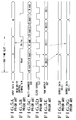
- Fig. 4 is a block diagram showing a main part of a conventional semiconductor memory device consisting of a synchronous RAM.
- the conventional semiconductor memory device includes a one-port RAM 49, a selector 48 for selectively inputting an address, a serial/parallel converter 50 for serial/parallel-converting an output from the RAM 49, a data input terminal 41 for inputting input data DI, a read/write terminal 42 for inputting an R/W (read/write) control signal R/W, a clock terminal 43 for inputting a clock signal CLK, a read address terminal 44 for inputting a read address RADD(N) where N is a positive integer of 2 or more, a read address terminal 45 for inputting a read address RADD(N-1), a write address terminal 46 for inputting a write address WADD, an address select terminal 47 for inputting an address select signal SEL, a data output terminal (N) 51 for outputting output data DO(N), a data output terminal (N-1) 52 for outputting output data DO(N-1), and a data output terminal (N-2) 53 for outputting output data DO(N-2).
- a clock signal CLK having a frequency of (N+1) times is input to the one-port RAM 49 within one time slot of input data in Fig. 5A, and even-numbered periods of the clock signal CLK are assigned to a read control signal as shown in Fig. 5B.
- N multi-addresses switched by the selector 48 are accessed, data output and controlled in a sequence [Read (N), Read (N-1),..., Write] as shown in Fig.
- FIG. 5E is serial/parallel-converted by the serial/parallel converter 50, and as shown in Figs. 5F and 5G, output data DO(N), DO(N-1),... are distributively output.
- Input data A and B shown in Fig. 5A are written at the period of the last clock signal CLK within one time slot in accordance with the control signal of Fig. 5B.
- a semiconductor memory device comprising N M-port RAMs (where each of M and N is a positive integer of not less than two) which are operated in synchronization with a common clock signal, a data input terminal for commonly inputting write data to data input terminals of the M-port RAMs, N ⁇ (M-1) read address terminals for independently inputting read addresses to first to (M-1)th port address terminals of the M-port RAMs, a write address terminal for commonly inputting a write address to Mth port address terminals of the M-port RAMs, and N ⁇ (M-1) data output terminals for independently outputting read data from data output terminals of the M-port RAMs.
- Fig. 1 shows a main part of the embodiment of the present invention and a basic arrangement of the present invention.
- a semiconductor memory device includes a synchronous M-port RAM(N) 8 (where each of M and N is a positive integer of 2 or more), a synchronous M-port RAM(N-1) 9, a synchronous M-port RAM(N-2) 10, and a synchronous M-port RAM(N-3) 11 which are operated in synchronization with a clock signal.
- An input terminal IN of each of the M-port RAM(N-1) 8, RAM(N-2) 9, RAM(N-2) 10, and RAM(N-3) 11 is connected to a data input terminal 1 for inputting input data DI
- first port address terminals P1 of the RAM(N), RAM(N-1), RAM(N-2), and RAM(N-3) 8, 9, 10, and 11 are connected to a read address terminal (N) 2 for inputting a read address RADD(N), a read address terminal (N-1) 3 for inputting a read address RADD(N-1), a read address terminal (N-2) 4 for inputting a read address RADD(N-2), and a read address terminal (N-3) 5 for inputting a read address RADD(N-3), respectively.
- Each Mth-port address terminal P M is connected to a write address terminal 6 for inputting a write address WADD, and each clock terminal CLK is connected to a clock terminal 7 for receiving a clock signal CLK.
- Output terminals OUT of the RAMs 8, 9, 10, and 11 are connected to a data output terminal (N) 12 for outputting output data DO(N), a data output terminal (N-1) 13 for outputting output data DO(N-1), a data output terminal (N-2) 14 for outputting output data DO(N-2), and a data output terminal (N-3) 15 for outputting output data DO(N-3), respectively.
- a semiconductor memory device includes a two-port RAM(2) 28 and a two-port RAM(1) 29.
- Input terminals IN of the two-port RAM(2) 28 and RAM(1) 29 are commonly connected to a data input terminal 21 for receiving input data DI
- first port address terminals P1 of the RAM(2) 28 and RAM(1) 29 are connected to a read address terminal (2) 22 for receiving a read address RADD(2) and a read address terminal (1) 23 for receiving a read address RADD(1), respectively.
- Second port address terminals P2 of the RAM(2) 28 and RAM(1) 29 are commonly connected to a write address terminal 26 for receiving a write address WADD, each clock terminal OUT is connected to a clock terminal 27 for receiving a clock signal CLK, and output terminals OUT of the RAM(2) 28 and RAM(1) 29 are connected to a data output terminal (2) 32 for outputting output data DO(2) and a data output terminal (1) 33 for outputting output data DO(1), respectively.
- the write address WADD is input from the write address terminal 26 to the two-port RAM(2) 28 and RAM(1) 29 as shown in Fig. 3D, and the same data DI which are represented as A and B in Fig. 3A are simultaneously written from the data input terminal 21 at the same address.
- the read address RADD(2) is input from the read address terminal (2) 22 to the two-port RAM(2) 28 as shown in Fig. 3B, and the read address RADD(1) different from the read address RADD(2) is input from the read address terminal (1) 23 to the two-port RAM(1) 29 as shown in Fig. 3C.
- the output data DO(2) is output from the two-port RAM(2) 28 to the data output terminal (2) 23 as shown in Fig. 3F, and the output data DO(1) different from the output data DO(2) is output from the two-port RAM(1) 29 to the data output terminal (1) 33 as shown in Fig. 3G.
- N ⁇ (M-1) the number of data which can be read at one clock timing is given as N ⁇ (M-1) in a general arrangement shown in Fig. 1.
- an arrangement in which three or more two-port RAMs are used is effective to simultaneously output a large number of data.
- N ⁇ (M-1) read address terminals and data output terminals which are independently arranged are connected to the first to (M-1)th port address terminals and the read data output terminals of N M-port RAMs which are operated in synchronization with a clock, and a write address terminal and a data input terminal are commonly connected to each of the Mth port address terminal and the Mth data input terminal.
- a high-performance RAM is not required, and the yield of LSIs can be increased.
Abstract
Description
- The present invention relates to a semiconductor memory device consisting of a synchronous RAM (Random Access Memory) which is used in a semiconductor memory device consisting of a synchronous RAM and, more particularly, is capable of simultaneously performing write access of the same data at an arbitrary address and read access of a plurality of data.
- Fig. 4 is a block diagram showing a main part of a conventional semiconductor memory device consisting of a synchronous RAM.
- The conventional semiconductor memory device includes a one-
port RAM 49, aselector 48 for selectively inputting an address, a serial/parallel converter 50 for serial/parallel-converting an output from theRAM 49, adata input terminal 41 for inputting input data DI, a read/writeterminal 42 for inputting an R/W (read/write) control signal R/W, aclock terminal 43 for inputting a clock signal CLK, aread address terminal 44 for inputting a read address RADD(N) where N is a positive integer of 2 or more, aread address terminal 45 for inputting a read address RADD(N-1), awrite address terminal 46 for inputting a write address WADD, an addressselect terminal 47 for inputting an address select signal SEL, a data output terminal (N) 51 for outputting output data DO(N), a data output terminal (N-1) 52 for outputting output data DO(N-1), and a data output terminal (N-2) 53 for outputting output data DO(N-2). - An operation of the conventional semiconductor memory device will be described below with reference to operation timing charts shown in Figs. 5A to 5G. Note that, for descriptive simplicity, Figs. 5A to 5G show a case wherein a condition N = 2 is satisfied.
- As shown in Fig. 4, when data at N different addresses are to be simultaneously extracted by a one-port RAM within one time slot, the following operation is performed. That is, as shown in Fig. 5D, a clock signal CLK having a frequency of (N+1) times is input to the one-
port RAM 49 within one time slot of input data in Fig. 5A, and even-numbered periods of the clock signal CLK are assigned to a read control signal as shown in Fig. 5B. As shown in Fig. 5C, N multi-addresses switched by theselector 48 are accessed, data output and controlled in a sequence [Read (N), Read (N-1),..., Write] as shown in Fig. 5E is serial/parallel-converted by the serial/parallel converter 50, and as shown in Figs. 5F and 5G, output data DO(N), DO(N-1),... are distributively output. Input data A and B shown in Fig. 5A are written at the period of the last clock signal CLK within one time slot in accordance with the control signal of Fig. 5B. - As described above, when an arrangement uses the conventional one-port RAM shown in Fig. 4, and data at N different addresses are to be simultaneously extracted within one time slot, a clock signal having a frequency of (N+1) times must be input to the one-port RAM within one time slot. When the frequency of the clock signal is increased, the RAM may not be operated, or a high-performance RAM is required. Therefore, the yield of LSIs is disadvantageously decreased.
- It is an object of the present invention to provide a semiconductor device capable of simultaneously performing write access of data at an arbitrary memory address and read access of a plurality of data without any increase in clock frequency.
- It is another object of the present invention to provide a semiconductor memory device requiring no high-performance RAM.
- In order to achieve the above objects, according to the present invention, there is provided a semiconductor memory device comprising N M-port RAMs (where each of M and N is a positive integer of not less than two) which are operated in synchronization with a common clock signal, a data input terminal for commonly inputting write data to data input terminals of the M-port RAMs, N × (M-1) read address terminals for independently inputting read addresses to first to (M-1)th port address terminals of the M-port RAMs, a write address terminal for commonly inputting a write address to Mth port address terminals of the M-port RAMs, and N × (M-1) data output terminals for independently outputting read data from data output terminals of the M-port RAMs.
- An embodiment of the present invention will be described below with reference to the accompanying drawings:
- Fig. 1 is a block diagram showing a semiconductor memory device according to an embodiment of the present invention;
- Fig. 2 is a block diagram showing a case wherein a condition N = M = 2 is satisfied in Fig. 1;
- Figs. 3A to 3G are timing charts for explaining an operation in Fig. 2;
- Fig. 4 is a block diagram showing a conventional semiconductor memory device; and
- Figs. 5A to 5G are timing charts for explaining an operation in Fig. 4.
- Fig. 1 shows a main part of the embodiment of the present invention and a basic arrangement of the present invention.
- According to the first embodiment of the present invention, a semiconductor memory device includes a synchronous M-port RAM(N) 8 (where each of M and N is a positive integer of 2 or more), a synchronous M-port RAM(N-1) 9, a synchronous M-port RAM(N-2) 10, and a synchronous M-port RAM(N-3) 11 which are operated in synchronization with a clock signal. An input terminal IN of each of the M-port RAM(N-1) 8, RAM(N-2) 9, RAM(N-2) 10, and RAM(N-3) 11 is connected to a
data input terminal 1 for inputting input data DI, and first port address terminals P₁ of the RAM(N), RAM(N-1), RAM(N-2), and RAM(N-3) 8, 9, 10, and 11 are connected to a read address terminal (N) 2 for inputting a read address RADD(N), a read address terminal (N-1) 3 for inputting a read address RADD(N-1), a read address terminal (N-2) 4 for inputting a read address RADD(N-2), and a read address terminal (N-3) 5 for inputting a read address RADD(N-3), respectively. Each Mth-port address terminal PM is connected to a write address terminal 6 for inputting a write address WADD, and each clock terminal CLK is connected to aclock terminal 7 for receiving a clock signal CLK. Output terminals OUT of theRAMs - Fig. 2 shows a case wherein a condition N = M = 2 is satisfied in Fig. 1.
- In this embodiment, a semiconductor memory device includes a two-port RAM(2) 28 and a two-port RAM(1) 29. Input terminals IN of the two-port RAM(2) 28 and RAM(1) 29 are commonly connected to a
data input terminal 21 for receiving input data DI, and first port address terminals P₁ of the RAM(2) 28 and RAM(1) 29 are connected to a read address terminal (2) 22 for receiving a read address RADD(2) and a read address terminal (1) 23 for receiving a read address RADD(1), respectively. Second port address terminals P₂ of the RAM(2) 28 and RAM(1) 29 are commonly connected to awrite address terminal 26 for receiving a write address WADD, each clock terminal OUT is connected to aclock terminal 27 for receiving a clock signal CLK, and output terminals OUT of the RAM(2) 28 and RAM(1) 29 are connected to a data output terminal (2) 32 for outputting output data DO(2) and a data output terminal (1) 33 for outputting output data DO(1), respectively. - An operation of this embodiment will be described below with reference to timing charts shown in Figs. 3A to 3G.
- In write access of data, the write address WADD is input from the
write address terminal 26 to the two-port RAM(2) 28 and RAM(1) 29 as shown in Fig. 3D, and the same data DI which are represented as A and B in Fig. 3A are simultaneously written from thedata input terminal 21 at the same address. - In read access of data, the read address RADD(2) is input from the read address terminal (2) 22 to the two-port RAM(2) 28 as shown in Fig. 3B, and the read address RADD(1) different from the read address RADD(2) is input from the read address terminal (1) 23 to the two-port RAM(1) 29 as shown in Fig. 3C. For this reason, the output data DO(2) is output from the two-port RAM(2) 28 to the data output terminal (2) 23 as shown in Fig. 3F, and the output data DO(1) different from the output data DO(2) is output from the two-port RAM(1) 29 to the data output terminal (1) 33 as shown in Fig. 3G.
- That is, according to this embodiment, as shown in Fig. 3E, different data can be read at one clock timing within one time slot. In this case, the number of data which can be read at one clock timing is given as N × (M-1) in a general arrangement shown in Fig. 1.
- In addition, when a condition N = M = 2 is satisfied in Fig. 1, since a two-port RAM is used, write access and read access can be simultaneously performed.
- In addition to the above embodiment, an arrangement in which three or more two-port RAMs are used is effective to simultaneously output a large number of data.
- As described above, according to the present invention, N × (M-1) read address terminals and data output terminals which are independently arranged are connected to the first to (M-1)th port address terminals and the read data output terminals of N M-port RAMs which are operated in synchronization with a clock, and a write address terminal and a data input terminal are commonly connected to each of the Mth port address terminal and the Mth data input terminal. With the above arrangement, the following advantage can be obtained. N × (M-1) data can be read at one clock timing within one time slot, and at the same time, the same data can be written at an arbitrary address.
- According to the present invention, a high-performance RAM is not required, and the yield of LSIs can be increased.
Claims (4)
- A semiconductor memory device characterized by comprising:
N M-port RAMs (8 - 11) (where each of M and N is a positive integer of not less than two) which are operated in synchronization with a common clock signal (CLK);
a data input terminal (1) for commonly inputting write data to data input terminals (IN) of said M-port RAMs;
N × (M-1) read address terminals (2 - 5) for independently inputting read addresses to first to (M-1)th port address terminals (P₁) of said M-port RAMs;
a write address terminal (6) for commonly inputting a write address to Mth port address terminals (PM) of said M-port RAMs; and
N × (M-1) data output terminals (12 - 15) for independently outputting read data from data output terminals (OUT) of said M-port RAMs. - A device according to claim 1, wherein a condition M = 2 is satisfied.
- A device according to claim 1, wherein a condition N = M = 2 is satisfied.
- A device according to claim 1, 2 or 3, wherein the clock signal has one clock timing within one time slot.
Applications Claiming Priority (2)
| Application Number | Priority Date | Filing Date | Title |
|---|---|---|---|
| JP183667/91 | 1991-06-27 | ||
| JP18366791A JP3169639B2 (en) | 1991-06-27 | 1991-06-27 | Semiconductor storage device |
Publications (3)
| Publication Number | Publication Date |
|---|---|
| EP0520425A2 true EP0520425A2 (en) | 1992-12-30 |
| EP0520425A3 EP0520425A3 (en) | 1995-03-22 |
| EP0520425B1 EP0520425B1 (en) | 1998-03-04 |
Family
ID=16139826
Family Applications (1)
| Application Number | Title | Priority Date | Filing Date |
|---|---|---|---|
| EP92110672A Expired - Lifetime EP0520425B1 (en) | 1991-06-27 | 1992-06-25 | Semiconductor memory device |
Country Status (5)
| Country | Link |
|---|---|
| US (1) | US5319596A (en) |
| EP (1) | EP0520425B1 (en) |
| JP (1) | JP3169639B2 (en) |
| CA (1) | CA2072046C (en) |
| DE (1) | DE69224559T2 (en) |
Cited By (7)
| Publication number | Priority date | Publication date | Assignee | Title |
|---|---|---|---|---|
| WO2000033315A1 (en) * | 1998-12-03 | 2000-06-08 | Sun Microsystems, Inc. | Apparatus and method for optimizing die utilization and speed performance by register file splitting |
| EP1220226A2 (en) * | 2000-12-20 | 2002-07-03 | Fujitsu Limited | Multi-port memory based on DRAM core |
| DE10350281A1 (en) * | 2003-10-28 | 2005-06-16 | Infineon Technologies Ag | Data processing device in which the memory write control signal is temporally independent of the memory read control signal |
| US7114056B2 (en) | 1998-12-03 | 2006-09-26 | Sun Microsystems, Inc. | Local and global register partitioning in a VLIW processor |
| US7117342B2 (en) | 1998-12-03 | 2006-10-03 | Sun Microsystems, Inc. | Implicitly derived register specifiers in a processor |
| US7120761B2 (en) | 2000-12-20 | 2006-10-10 | Fujitsu Limited | Multi-port memory based on DRAM core |
| CN1734668B (en) * | 2000-12-20 | 2010-05-05 | 富士通微电子株式会社 | Multi-port memory based on dram core |
Families Citing this family (5)
| Publication number | Priority date | Publication date | Assignee | Title |
|---|---|---|---|---|
| US5436863A (en) * | 1993-04-26 | 1995-07-25 | Nec Corporation | Semiconductor memory device |
| JPH0713847A (en) * | 1993-04-26 | 1995-01-17 | Nec Corp | Semiconductor storage device |
| WO1996007139A1 (en) * | 1994-09-01 | 1996-03-07 | Mcalpine Gary L | A multi-port memory system including read and write buffer interfaces |
| JPH1168797A (en) * | 1997-08-26 | 1999-03-09 | Nec Corp | Variable length cell correspondent phase changing device |
| US9076553B2 (en) | 2013-11-13 | 2015-07-07 | Taiwan Semiconductor Manufacturing Company Limited | SPSRAM wrapper |
Citations (6)
| Publication number | Priority date | Publication date | Assignee | Title |
|---|---|---|---|---|
| US4616310A (en) * | 1983-05-20 | 1986-10-07 | International Business Machines Corporation | Communicating random access memory |
| US4893279A (en) * | 1986-03-04 | 1990-01-09 | Advanced Micro Devices Inc. | Storage arrangement having a pair of RAM memories selectively configurable for dual-access and two single-access RAMs |
| US4912680A (en) * | 1987-09-03 | 1990-03-27 | Minolta Camera Kabushiki Kaisha | Image memory having plural input registers and output registers to provide random and serial accesses |
| EP0375194A2 (en) * | 1988-12-19 | 1990-06-27 | Advanced Micro Devices, Inc. | Dual port RAM |
| EP0374829A2 (en) * | 1988-12-19 | 1990-06-27 | Bull HN Information Systems Inc. | Dual port memory unit |
| EP0434852A1 (en) * | 1989-12-23 | 1991-07-03 | International Business Machines Corporation | Highly integrated multi-port semiconductor storage |
Family Cites Families (2)
| Publication number | Priority date | Publication date | Assignee | Title |
|---|---|---|---|---|
| JPS59151371A (en) * | 1983-02-03 | 1984-08-29 | Toshiba Corp | Semiconductor memory element |
| JPS62272352A (en) * | 1986-05-21 | 1987-11-26 | Matsushita Graphic Commun Syst Inc | Memory control circuit |
-
1991
- 1991-06-27 JP JP18366791A patent/JP3169639B2/en not_active Expired - Fee Related
-
1992
- 1992-06-23 US US07/902,719 patent/US5319596A/en not_active Expired - Fee Related
- 1992-06-23 CA CA002072046A patent/CA2072046C/en not_active Expired - Fee Related
- 1992-06-25 DE DE69224559T patent/DE69224559T2/en not_active Expired - Fee Related
- 1992-06-25 EP EP92110672A patent/EP0520425B1/en not_active Expired - Lifetime
Patent Citations (6)
| Publication number | Priority date | Publication date | Assignee | Title |
|---|---|---|---|---|
| US4616310A (en) * | 1983-05-20 | 1986-10-07 | International Business Machines Corporation | Communicating random access memory |
| US4893279A (en) * | 1986-03-04 | 1990-01-09 | Advanced Micro Devices Inc. | Storage arrangement having a pair of RAM memories selectively configurable for dual-access and two single-access RAMs |
| US4912680A (en) * | 1987-09-03 | 1990-03-27 | Minolta Camera Kabushiki Kaisha | Image memory having plural input registers and output registers to provide random and serial accesses |
| EP0375194A2 (en) * | 1988-12-19 | 1990-06-27 | Advanced Micro Devices, Inc. | Dual port RAM |
| EP0374829A2 (en) * | 1988-12-19 | 1990-06-27 | Bull HN Information Systems Inc. | Dual port memory unit |
| EP0434852A1 (en) * | 1989-12-23 | 1991-07-03 | International Business Machines Corporation | Highly integrated multi-port semiconductor storage |
Cited By (15)
| Publication number | Priority date | Publication date | Assignee | Title |
|---|---|---|---|---|
| US7114056B2 (en) | 1998-12-03 | 2006-09-26 | Sun Microsystems, Inc. | Local and global register partitioning in a VLIW processor |
| US6343348B1 (en) | 1998-12-03 | 2002-01-29 | Sun Microsystems, Inc. | Apparatus and method for optimizing die utilization and speed performance by register file splitting |
| US7117342B2 (en) | 1998-12-03 | 2006-10-03 | Sun Microsystems, Inc. | Implicitly derived register specifiers in a processor |
| WO2000033315A1 (en) * | 1998-12-03 | 2000-06-08 | Sun Microsystems, Inc. | Apparatus and method for optimizing die utilization and speed performance by register file splitting |
| EP1220226A3 (en) * | 2000-12-20 | 2002-12-18 | Fujitsu Limited | Multi-port memory based on DRAM core |
| EP1220226A2 (en) * | 2000-12-20 | 2002-07-03 | Fujitsu Limited | Multi-port memory based on DRAM core |
| US7120761B2 (en) | 2000-12-20 | 2006-10-10 | Fujitsu Limited | Multi-port memory based on DRAM core |
| CN1734668B (en) * | 2000-12-20 | 2010-05-05 | 富士通微电子株式会社 | Multi-port memory based on dram core |
| CN101452737B (en) * | 2000-12-20 | 2011-02-02 | 富士通半导体股份有限公司 | Multiport memory based on dynamic random access memory core |
| US7911825B2 (en) | 2000-12-20 | 2011-03-22 | Fujitsu Semiconductor Ltd. | Multi-port memory based on DRAM core |
| US20130201751A1 (en) * | 2000-12-20 | 2013-08-08 | Fujitsu Semiconductor Limited | Multi-port memory based on dram core |
| US8547776B2 (en) | 2000-12-20 | 2013-10-01 | Fujitsu Semiconductor Limited | Multi-port memory based on DRAM core |
| US8687456B2 (en) | 2000-12-20 | 2014-04-01 | Fujitsu Semiconductor Limited | Multi-port memory based on DRAM core |
| US8717842B2 (en) | 2000-12-20 | 2014-05-06 | Fujitsu Semiconductor Limited | Multi-port memory based on DRAM core |
| DE10350281A1 (en) * | 2003-10-28 | 2005-06-16 | Infineon Technologies Ag | Data processing device in which the memory write control signal is temporally independent of the memory read control signal |
Also Published As
| Publication number | Publication date |
|---|---|
| DE69224559D1 (en) | 1998-04-09 |
| EP0520425B1 (en) | 1998-03-04 |
| JP3169639B2 (en) | 2001-05-28 |
| JPH05100946A (en) | 1993-04-23 |
| EP0520425A3 (en) | 1995-03-22 |
| DE69224559T2 (en) | 1998-07-23 |
| CA2072046C (en) | 1997-12-09 |
| CA2072046A1 (en) | 1992-12-28 |
| US5319596A (en) | 1994-06-07 |
Similar Documents
| Publication | Publication Date | Title |
|---|---|---|
| US4825411A (en) | Dual-port memory with asynchronous control of serial data memory transfer | |
| EP0401340B1 (en) | Method and apparatus for handling high speed data | |
| US5390149A (en) | System including a data processor, a synchronous dram, a peripheral device, and a system clock | |
| US5416749A (en) | Data retrieval from sequential-access memory device | |
| EP0345807B1 (en) | Line memory for speed conversion | |
| EP0520425A2 (en) | Semiconductor memory device | |
| US5406132A (en) | Waveform shaper for semiconductor testing devices | |
| US4903240A (en) | Readout circuit and method for multiphase memory array | |
| US5508967A (en) | Line memory | |
| EP0290042A2 (en) | Memory circuit with improved serial addressing scheme | |
| EP0589662A2 (en) | Digital signal processing system | |
| US4503525A (en) | Common circuit for dynamic memory refresh and system clock function | |
| JP2627903B2 (en) | Semiconductor storage device | |
| EP0342022B1 (en) | Image data read out sytem in a digital image processing system | |
| JPS603714B2 (en) | variable length shift register | |
| EP1459291B1 (en) | Digital line delay using a single port memory | |
| CA1191211A (en) | Electronic time switch | |
| EP1050883B1 (en) | Circuits for controlling the storage of data into memory | |
| KR200155054Y1 (en) | Counter circuit | |
| KR0182037B1 (en) | Over sampling digital filter | |
| JPH07107706B2 (en) | Line buffer with variable number of delay stages | |
| JP3188287B2 (en) | Service tone generation method | |
| KR0181485B1 (en) | Data-buffering device for data telecommunication | |
| RU1783537C (en) | Device for connection of sources of information to common trunk line | |
| SU1133622A1 (en) | Buffer storage |
Legal Events
| Date | Code | Title | Description |
|---|---|---|---|
| PUAI | Public reference made under article 153(3) epc to a published international application that has entered the european phase |
Free format text: ORIGINAL CODE: 0009012 |
|
| AK | Designated contracting states |
Kind code of ref document: A2 Designated state(s): DE FR GB |
|
| PUAL | Search report despatched |
Free format text: ORIGINAL CODE: 0009013 |
|
| AK | Designated contracting states |
Kind code of ref document: A3 Designated state(s): DE FR GB |
|
| 17P | Request for examination filed |
Effective date: 19950210 |
|
| 17Q | First examination report despatched |
Effective date: 19960424 |
|
| GRAG | Despatch of communication of intention to grant |
Free format text: ORIGINAL CODE: EPIDOS AGRA |
|
| GRAG | Despatch of communication of intention to grant |
Free format text: ORIGINAL CODE: EPIDOS AGRA |
|
| GRAG | Despatch of communication of intention to grant |
Free format text: ORIGINAL CODE: EPIDOS AGRA |
|
| GRAH | Despatch of communication of intention to grant a patent |
Free format text: ORIGINAL CODE: EPIDOS IGRA |
|
| GRAH | Despatch of communication of intention to grant a patent |
Free format text: ORIGINAL CODE: EPIDOS IGRA |
|
| GRAA | (expected) grant |
Free format text: ORIGINAL CODE: 0009210 |
|
| AK | Designated contracting states |
Kind code of ref document: B1 Designated state(s): DE FR GB |
|
| REF | Corresponds to: |
Ref document number: 69224559 Country of ref document: DE Date of ref document: 19980409 |
|
| ET | Fr: translation filed | ||
| PLBE | No opposition filed within time limit |
Free format text: ORIGINAL CODE: 0009261 |
|
| STAA | Information on the status of an ep patent application or granted ep patent |
Free format text: STATUS: NO OPPOSITION FILED WITHIN TIME LIMIT |
|
| 26N | No opposition filed | ||
| PGFP | Annual fee paid to national office [announced via postgrant information from national office to epo] |
Ref country code: FR Payment date: 20010611 Year of fee payment: 10 |
|
| PGFP | Annual fee paid to national office [announced via postgrant information from national office to epo] |
Ref country code: DE Payment date: 20010618 Year of fee payment: 10 |
|
| PGFP | Annual fee paid to national office [announced via postgrant information from national office to epo] |
Ref country code: GB Payment date: 20010620 Year of fee payment: 10 |
|
| REG | Reference to a national code |
Ref country code: GB Ref legal event code: IF02 |
|
| PG25 | Lapsed in a contracting state [announced via postgrant information from national office to epo] |
Ref country code: GB Free format text: LAPSE BECAUSE OF NON-PAYMENT OF DUE FEES Effective date: 20020625 |
|
| PG25 | Lapsed in a contracting state [announced via postgrant information from national office to epo] |
Ref country code: DE Free format text: LAPSE BECAUSE OF NON-PAYMENT OF DUE FEES Effective date: 20030101 |
|
| GBPC | Gb: european patent ceased through non-payment of renewal fee |
Effective date: 20020625 |
|
| PG25 | Lapsed in a contracting state [announced via postgrant information from national office to epo] |
Ref country code: FR Free format text: LAPSE BECAUSE OF NON-PAYMENT OF DUE FEES Effective date: 20030228 |
|
| REG | Reference to a national code |
Ref country code: FR Ref legal event code: ST |