US4458357A - Circuit board identity generator - Google Patents
Circuit board identity generator Download PDFInfo
- Publication number
- US4458357A US4458357A US06/293,503 US29350381A US4458357A US 4458357 A US4458357 A US 4458357A US 29350381 A US29350381 A US 29350381A US 4458357 A US4458357 A US 4458357A
- Authority
- US
- United States
- Prior art keywords
- counter means
- circuit boards
- counter
- identity
- enabled
- Prior art date
- Legal status (The legal status is an assumption and is not a legal conclusion. Google has not performed a legal analysis and makes no representation as to the accuracy of the status listed.)
- Expired - Fee Related
Links
Images


Classifications
-
- G—PHYSICS
- G06—COMPUTING; CALCULATING OR COUNTING
- G06F—ELECTRIC DIGITAL DATA PROCESSING
- G06F12/00—Accessing, addressing or allocating within memory systems or architectures
- G06F12/02—Addressing or allocation; Relocation
- G06F12/06—Addressing a physical block of locations, e.g. base addressing, module addressing, memory dedication
- G06F12/0646—Configuration or reconfiguration
- G06F12/0669—Configuration or reconfiguration with decentralised address assignment
- G06F12/0676—Configuration or reconfiguration with decentralised address assignment the address being position dependent
Definitions
- the present invention is related to apparatus for automatically producing a unique identification code for a number of circuit boards in an electronic system.
- many computer systems employ a plurality of similar electronic subsystems, such as a plurality of input/output devices, a plurality of microprocessors, and the like.
- these computer systems employ such plural subsystems, it is necessary to identify each of the individual electronic subsystems to enable the computing system to selectively choose a unique electronic subsystem when necessary.
- peripheral devices such as disc drives, printers, and the like. It is therefore necessary that each of the peripheral devices be uniquely identifiable by the computer system, such that an individual peripheral device may be selected for an operation.
- circuitry associated with each disc must provide an individual identification number such that each disc drive can be uniquely identified and chosen by the computing system.
- Usual prior art techniques of identifying the various subsystems include the use of a "strap" circuit or a “switch” circuit.
- the strap or switch circuit is provided on the circuit board of each subsystem to be identified. Both types of circuits provide a plurality of identification bit lines, each of the bit lines providing either a logical high ("1") or logical low (“0") level, the combination of the plurality of identification bit lines producing an identification number (i.e., "1011") unique to the particular apparatus.
- each of the individual identification bit lines is permanently attached or "strapped" to either the logical high or logical low level, while the switch circuits selectively apply each of the individual identity bit lines to either the logical high or logical low level via individual thumb-wheel or toggle switches, the switches being manually set to provide any particular identification number.
- the logical high and low levels are usually taken from the positive supply voltage and ground potential, respectively.
- switch circuit technique for providing the identification is more flexible than the strap circuit technique, similar problems exist insofar as two or more computer subsystem circuit boards may potentially be provided with the same identification number. Further, the use of thumb-wheel or toggle switches to provide an identification number is far from reliable, and requires the manual adjustment of each and every computer subsystem circuit requiring identification.
- the "first" subsystem may be identified as “subsystem No. 21,” the second as “subsystem No. 9,” and so on, in no particular sequential order.
- a random technique can provide the unique identification of circuit elements, random numbering increases software overhead and requirements such as software reference range.
- circuit board identification generators on a plurality of computer subsystem circuit boards, the circuit board identification generators being designed and interconnected so as to automatically and sequentially identify each of the circuit boards with a unique identification number.
- the circuit board identity generators identify each computer subsystem automatically upon turning on the computer system.
- each circuit board in a system includes an identity generator which is enabled and disabled at preselected times to provide a unique code identifying each circuit board. More specifically, each identity generator is successively enabled and thereafter all identity generators are simultaneously disabled to provide the unique identification code.
- each of the circuit board identity generators includes counter means for counting in accordance with a clock signal when enabled for providing a count output.
- Circuitry is provided for automatically enabling the counter means in each of the identity generators in a predetermined succession, and for automatically disabling the counter means in each of the identity generators at substantially the same time, whereby the count output from each of the identity generators provides a unique identification number for an associated one of the circuit boards.
- the circuity for automatically enabling the counter means in each of the identity generators successively enables the counter means approximately one clock signal period after the counter means in the preceding identity generator is enabled, and the circuitry for automatically disabling the counter means in each of the identity generators disables the counter means substantially within one or two periods of the clock signal after the counter means in all of the identity generators are enabled.
- the disabling circuitry disables the counter means within one period of the clock signal, N circuit boards will be identified as circuit boards "N-1" through "0".
- the circuitry for automatically disabling the counter means disables the counter means within two periods of the clock signal, N circuit boards will be identified as circuit boards "N" through “1".
- the circuitry for enabling and disabling the counter means comprises logic means receiving system signals from a common circuit for providing an enable signal in accordance with the system signal.
- the counter means includes (i) an enable input receiving the enable signal for selectively enabling and disabling the counter means in accordance therewith, (ii) a clock input receiving a clock signal from the system, and (iii) a count output.
- the counter means is selectively enabled and disabled at predetermined times, the counter means counting in accordance with the clock signal when enabled, the count output of the counter means providing the identification number.
- the counter means further includes presetting means for presetting the count output to a preselected number and an indication output signal applied to the common circuit for indicating that the count output of the counter is at the preselected number.
- the counter means is preset to the preselected number by the presetting means before being enabled and counts from the preselected number in accordance with the clock signal when enabled.
- a circuit board identification system is provided with a common circuit, and a succession of circuit boards to be identified connected to the common circuit, each of the circuit boards being provided with one of the circuit board identity generators.
- the common circuit includes a first bus for supplying a signal to the preset input of each of the counters, a second bus for supplying a clock signal to the clock input of the counters, a third bus providing a count terminate signal derived from the indication output signal from the counter in the last of the succession of circuit boards to the logic means of each of the counters, and a plurality of chain buses, the indication output from the counters in each of the circuit boards except the last of the succession of circuit boards being applied to the logic means of a succeeding counter via an associated one of the chain buses.
- the counters in each of the circuit boards are automatically enabled in a predetermined succession and automatically disabled in substantial time coincidence, whereby the count output from each of the counters provides a unique identification number for an associated one of the circuit boards.
- the logic means in accordance with the present invention may comprise a single two input logic gate, such as a NAND gate, or may be comprised of a delay type flip-flop which receives the count terminate signal and provides a delay output and a two input logic gate which receives the delay output.
- the output of the NAND gate provides the enable and disable signals to the counting means.
- the counting means in accordance with the present invention may comprise a single digital counter integrated circuit such as the Texas Instruments 74191, or may comprise two or more of such digital counters connected in cascade to thereby increase the number of circuit boards which may be identified.
- FIG. 1 is a schematic illustration of a prior art "strap" circuit for providing a unique circuit board identification number
- FIG. 2 is a schematic illustration of a prior art "switch" circuit for providing a unique circuit board identification number
- FIG. 3 is a block diagram illustrating the interconnections of a plurality of circuit board identification generators for providing a unique and sequential circuit board identification number for each of the circuit boards in accordance with the present invention
- FIG. 4 is a block diagram illustrating the details of one embodiment of the circuit board identity generator used on each circuit board in accordance with the present invention
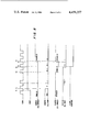
- FIG. 5 is a waveform diagram helpful in understanding the operation of the circuit board identity generators of FIGS. 3 and 4;
- FIG. 6 is a schematic diagram illustrating a technique for employing the circuit board identification number to identify a unique circuit board
- FIG. 7 is a block diagram illustrating a modification to the circuit board identity generators to provide both an extended range for the identification number and for insuring that the lowest numbered circuit board will be identified as board "1";
- FIG. 8 is a waveform diagram helpful in understanding the operation of the circuit board identity generator shown in FIG. 7.
- Circuit board X is identified within the system by providing a plurality of circuit board identification lines 2, each of the lines being permanently connected or “strapped” to either the 5 volt supply bus 4 or ground potential bus 6.
- the board identification lines 2 provide a unique binary word or number ("1011" shown in FIG. 1) by which the board can be identified, the lines applied to the 5 volt supply bus 4 being logical "1,” the lines applied to ground potential bus 6 being logical "0.”
- FIG. 2 illustrates a prior art switch circuit, whereby each of the circuit board identification lines 2 are selectively applied to either the 5 volt supply bus 4 or ground potential bus 6 via switches SWl-SWn.
- the switches SWl-SWn are usually thumb-wheel or toggle switches, and are manually set by the operator to provide any particular circuit board identification number.
- FIGS. 1 and 2 While use of the prior art devices illustrated in FIGS. 1 and 2 may be acceptable for very small systems, it can be seen that as the number of circuit boards which must be identified increases, the amount of maintenance required by the identification circuitry increases. That is, in the FIG. 1 arrangement, each of the circuit boards must be manually "strapped" to the supply buses 4 and 6, while in FIG. 2, each of the circuit boards must be manually switched to the buses to provide the appropriate board identification numbers. Clearly, this manual intervention causes problems in reliability due to human error. Also, since the strap circuit technique of FIG. 1 is a permanent circuit modification, such technique is highly inflexible. Finally, while each of the circuit boards wired in accordance with the prior art techniques of FIGS. 1 and 2 may be provided with a unique circuit board identification number, the identification numbers do not necessarily have to be sequential. The use of nonsequential identification numbers results in a decreased software reference range for the circuit boards, and increased software overhead to account therefor.
- FIG. 3 illustrates a plurality of circuit boards each having a circuit board identification generator provided in accordance with the present invention, and the interconnections therebetween.
- the circuit boards referred to herein may be from any particular electronic subsystem.
- the circuit boards may be controllers for input/output devices such as discs, tape drives, etc., the circuit board identity generators providing a unique sequential identification number for each of the input/output devices.
- the circuit boards may each be disposed on an associated one of a plurality of identical microprocessors in a multiprocessing system, each of the circuit board identity generators providing a unique and sequential identification number for each of the microprocessors.
- N circuit boards are interconnected via clock bus 8, reset bus 10, count terminate bus 12 and chain buses a through (n-1), the buses being provided on a common backplane 18.
- Each circuit board has an associated circuit board identification generator a through n located therein, the circuit board identification generators occupying only a small portion of the associated circuit board.
- Each circuit board identification generator includes NAND gate 20, counter 22, and inverter 24, the reference numerals for elements 20, 22 and 24 identifying the particular circuit board identification generator, a through n, with which the element is associated, NAND gate 20a being disposed in generator a, NAND gate 20b being disposed in generator b, and so on.
- An additional inverter 26 is provided in the backplane 18.
- the system RESET and system CLOCK signals are applied to the LOAD and CLOCK inputs, respectively, of counters 22a-22n via system RESET bus 10 and CLOCK bus 8.
- the counters 22a-22n receive ENABLE signals from the respective NAND gates 20a-20n.
- Counters 22a, 22b and 22n provide an identification number on identification lines 28a, 28b, and 28n, respectively, and a MAXIMUM COUNT output which goes high whenever the associated counter attains its maximum count.
- the MAXIMUM COUNT outputs from generators a through (n-1) are applied to associated chain buses via inverters 24a through 24 (n-1), the output of inverter 24a providing the input to chain bus a, the output of inverter 24b providing the input to chain bus b, and so on.
- the last generator, generator n applies its MAXIMUM COUNT output to the additional inverter 26 in the backplane 18, via inverter 24n, the output of inverter 26 being applied to the count terminate bus 12.
- NAND gates 20a-20n each receive a first input directly from count terminate bus 12.
- All NAND gates except NAND gate 20a in the first generator, generator a receive their second inputs from the inverted MAXIMUM COUNT output from the previous generator via the associated chain bus, NAND gate 20b receiving the inverted MAXIMUM COUNT output from generator a via chain bus a, NAND gate 20n receiving the inverted MAXIMUM COUNT output from generator n-1 via chain bus n-1. All of the NAND gates 20a-20n also receive a high signal level at the second inputs thereof from voltage supply V cc via resistors R. Since the second input to NAND gate 20a in generator a does not receive an inverted MAXIMUM COUNT signal, the second input thereof is constantly at a high level due to the supply voltage applied thereto.
- An individual circuit board identification generator (generator k, for example) essentially comprises a synchronous counter 22k having a MAXIMUM COUNT output and preset input, such as the Texas Instruments 74191 integrated circuit 22k.
- the counter 22k is a four-bit counter which may be preset according to the levels applied to the A-D inputs of pins 15, 1, 10 and 9, respectively, upon a negative going LOAD pulse. Since each of the inputs A-D is tied to the positive voltage supply via resistor R, the count of counter 22k will be preset to "1111" upon a negative-going transistion of the LOAD pulse.
- This preset count causes the Q 0 -Q 3 outputs on pins 3, 2, 6 and 7, respectively, to produce the number "1111” on identification ouput lines 28k, and also causes the MAXIMUM COUNT indication on pin 12 to go high to indicate that the maximum count has been attained.
- the counter will begin counting at the positive going transistions of the system CLOCK applied to the CLOCK input at pin 14 whenever the ENABLE input from NAND gate 20k applied to pin 4 attains a low value and the LOAD pulse switches to a high state.
- Pin 5 is tied to ground to thereby cause the counter 22k to count up, the counter after "1111” being "0000,” the next being "0001,” and so on.
- the RESET line provides a low signal level to the LOAD input of counters 22a-22n to thereby load the maximum count into each of the counters as illustrated at time T 1 , FIG. 5. Consequently, the MAXIMUM COUNT output from each of the counters 22a-22n is high, and the inverted low signal is applied to the chain buses between each of the boards Since a low signal is applied to one of the inputs of each of NAND gates 20b-20n, the outputs of the associated NAND gates are driven high to thereby disable the associated counters 22b-22n.
- a high signal level from the output of inverter 26 is applied to the other input of the NAND gates 20a-20n when the counter 22n is at its maximum count. Since the one input to NAND gate 20a is constantly held high, unlike NAND gate 20a cause the gate to provide a low signal level to counter 22a to enable the counter 22a as shown in FIG. 5.
- the LOAD signal may be released at time T 2 at least 35 ns prior to the rising edge of the clock signal at T 3 .
- Counter 22a responds at time T 3 to the positive edge of the CLOCK signal to count up from the maximum count to a zero count.
- the MAXIMUM COUNT output from counter 22a goes low and the inverted high level signal is applied to chain bus a.
- the output of NAND gate 20b goes low to enable counter 22b shortly after time T 3 , at time T 4 .
- Counter 22b now being enabled, responds at time T 5 to the positive transition of the CLOCK input to count up from the maximum back to the zero count.
- Counter 22a still enabled, counts from 0 to 1.
- counter 22a in the first generator will have achieved a count of N-4
- counter 22b in the next generator b will have achieved a count of N-5
- the counter in the next to the last generator will begin its count from its maximum to zero thereby enabling counter 22n at T 8 in a manner identical to that described for generators a and b. Since counter 22n is enabled, it responds to the rising edge of the CLOCK signal at time T 9 to count from its maximum count to a zero count.
- the MAXIMUM COUNT output from counter 22n achieves a low state, and soon thereafter, this low state is applied to the count terminate bus 12 via inverters 24n and 26.
- the low going COUNT TERMINATE signal is applied to each of the NAND gates 20a-20n at time T 10 to provide a high signal to the ENABLE input of each of the counters 22a-22n, thereby disabling all counters.
- each of the N generators a-n provide sequential identification numbers N-1 through zero, respectively, the identification numbers being available on identification lines 28a-28n.
- FIG. 6 illustrates one technique for using the identification number to produce an identification signal upon request.
- Each of the N circuit boards may be provided with exclusive OR gates 28-34, each of the exclusive OR gates receiving one of the identification lines at first inputs thereof.
- An identification request is applied to an identification request bus 36 common to all boards, the corresponding bits in the identification request bus being applied to the other input of the associated exclusive OR gates 28-34. Whenever the identification number exactly matches the identification request, the output from all exclusive OR gates 28-34 will be low, thereby providing a high output from NOR gate 38 indicating the location of the requested circuit board.
- FIG. 7 illustrates a circuit board identity generator which has been modified to provide an eight bit identification number, and further modified to number N boards from N to 1, rather than from (N-1) to 0.
- a pair of 74191 counters 40 and 42 are cascaded and have their PRESET inputs A-D tied to the positive 5 volt supply via resistor R1 to thereby preset the counters to the MAXIMUM COUNT of "1111" when the RESET signal, applied to the LOAD input of the counters, attains a low value.
- the Q 0 -Q 3 outputs from counter 40 are combined with the outputs "Q 4 -Q 7 ", to form identification lines 44.
- the signal on the chain bus from the previous generator is applied to a first input of NAND gate 48, the first input to NAND gate 48 also receiving the supply voltage via resistor R2.
- the system RESET signal is directly applied to the LOAD inputs of counters 40 and 42.
- the signal on the count terminate bus is applied to the D input of delay type flip-flop 50 which may be the 74S74 Dual D Positive Edge Triggered Flip Flop with preset and.clear.
- the system CLOCK is applied to the CLOCK input of flip-flop 50, while the CLEAR and PRESET inputs to the flip-flop are tied to the supply voltage via resistors R3 and R1, respectively.
- the Q output of flip-flop 50 is applied to the second input of NAND gate 48, the output of the latter being applied to the ENABLE inputs of counters 40 and 42.
- the system CLOCK is applied to the CLOCK input of counter 40, while the RIPPLE CLOCK output from pin 13 of counter 40 is applied to the CLOCK input of counter 42.
- the up/down mode inputs to counters 40 and 42 are tied to ground to provide a "count up" function for both counters, and the MAXIMUM COUNT outputs from counters 40 and 42 are applied to respective first and second inputs to NAND gate 52 which provides a chain bus output to the next succeeding circuit board identification generator.
- the counters 40 and 42 are cascaded by applying the RIPPLE CLOCK output from pin 13 of counter 40, which provides a negative going pulse for one half of the CLOCK whenever the maximum count (overflow) is reached by counter 40, to counter 42.
- the combination of counters 40 and 42 function as an eight bit counter. It is readily apparent that more than two of the counters can be cascaded in this manner to provide an arbitrarily large identification number to accommodate a large number of circuit boards.
- the delay type flip-flop 50 is provided to insure that the identification number of the last generator is "1", rather than "0". It should be noted that the flip-flop may be provided for this purpose in either the generators of FIGS. 4 or 7. Similarly, the cascaded counters shown in FIG. 7 may be used without the flip-flop to merely extend the counting range without affecting the value of the lowest identification number.
- counter 22n eventually becomes enabled at time T 3 , at which time counter 22a has attained the count of N-2.
- Counter 22n responds to the positive going CLOCK pulse at time T 4 by counting from the MAXIMUM COUNT to 0. Shortly there after, at time T 5 , a low going COUNT TERMINATE signal is applied to the count terminate bus.
- Each of the delay type flip-flops 50 in the associated generators receive the low going COUNT TERMINATE signal from the count terminate bus.
- the flip-flops 50 respond to the next positive going edge of the CLOCK signal by transfering the low going signal applied to the D input of the flip-flop to the Q output.
- each of the flip-flops 50 causes the output of NAND gate 48 to go high to thereby disable all of the counters 22a-22n at time T 7 .
- each of the counters 22a-22n is incremented at time T 6 , counter 22n counting from 0 to 1, counter 22a counting from N-1 to N.
- the highest numbered board has an identification number equal to "N”
- the lowest numbered board an identification number equal to "1”
- the inverter 26 may be located on a circuit board, rather than the backplane 18. Such a circuit board will always be identified with the lowest number but can be attached to the backplane at a number of locations. On the other hand, in the arrangement of FIG. 3, the lowest numbered circuit board must be placed in the backplane at the location of inverter 26, but all generators are identical.
Abstract
Description
Claims (14)
Priority Applications (1)
| Application Number | Priority Date | Filing Date | Title |
|---|---|---|---|
| US06/293,503 US4458357A (en) | 1981-08-17 | 1981-08-17 | Circuit board identity generator |
Applications Claiming Priority (1)
| Application Number | Priority Date | Filing Date | Title |
|---|---|---|---|
| US06/293,503 US4458357A (en) | 1981-08-17 | 1981-08-17 | Circuit board identity generator |
Publications (1)
| Publication Number | Publication Date |
|---|---|
| US4458357A true US4458357A (en) | 1984-07-03 |
Family
ID=23129357
Family Applications (1)
| Application Number | Title | Priority Date | Filing Date |
|---|---|---|---|
| US06/293,503 Expired - Fee Related US4458357A (en) | 1981-08-17 | 1981-08-17 | Circuit board identity generator |
Country Status (1)
| Country | Link |
|---|---|
| US (1) | US4458357A (en) |
Cited By (19)
| Publication number | Priority date | Publication date | Assignee | Title |
|---|---|---|---|---|
| EP0179497A2 (en) * | 1984-03-23 | 1986-04-30 | Philips Electronics Uk Limited | Electrical circuit arrangement and electrical circuit unit including an address generator for use in such an arrangement |
| EP0209923A1 (en) * | 1985-06-06 | 1987-01-28 | Koninklijke Philips Electronics N.V. | Arrangement for identifying peripheral apparatuses which may be connected at geographically different locations to a communication network by means of local coupling units |
| EP0216431A2 (en) * | 1985-09-27 | 1987-04-01 | Philips Electronics Uk Limited | Generating addresses for circuit units |
| US4774718A (en) * | 1987-07-24 | 1988-09-27 | Esm International Inc. | Automatic ejector rate normalizer |
| US4890262A (en) * | 1987-01-14 | 1989-12-26 | Texas Instruments Incorporated | Semiconductor memory with built-in defective bit relief circuit |
| US4984213A (en) * | 1989-02-21 | 1991-01-08 | Compaq Computer Corporation | Memory block address determination circuit |
| US5038320A (en) * | 1987-03-13 | 1991-08-06 | International Business Machines Corp. | Computer system with automatic initialization of pluggable option cards |
| FR2675605A1 (en) * | 1991-04-19 | 1992-10-23 | Alcatel Business Systems | METHOD AND DEVICE FOR ADDRESSING PERIPHERALS FOR SHARING A DATA TRANSMISSION CHANNEL BETWEEN PERIPHERALS. |
| US5237674A (en) * | 1987-04-11 | 1993-08-17 | Apple Computer, Inc. | Self identifying scheme for memory module including circuitry for identfying accessing speed |
| US5278958A (en) * | 1988-01-27 | 1994-01-11 | Kabushiki Kaisha Toshiba | Method and apparatus for selecting a keyboard on a computer system |
| US5341316A (en) * | 1989-09-08 | 1994-08-23 | Kabushiki Kaisha Toshiba | Personal computer system allowing selective use of built-in and external keyboards by means of selector |
| US5426767A (en) * | 1987-08-03 | 1995-06-20 | Compaq Computer Corporation | Method for distinguishing between a 286-type central processing unit and a 386-type central processing unit |
| US5699554A (en) * | 1994-10-27 | 1997-12-16 | Texas Instruments Incorporated | Apparatus for selective operation without optional circuitry |
| US5732280A (en) * | 1994-07-15 | 1998-03-24 | International Business Machines Corp. | Method and apparatus for dynamically assigning programmable option select identifiers |
| US5925113A (en) * | 1995-05-15 | 1999-07-20 | Hyundai Electronics Industries Co., Ltd. | Burst mode end detection unit |
| US5928343A (en) * | 1990-04-18 | 1999-07-27 | Rambus Inc. | Memory module having memory devices containing internal device ID registers and method of initializing same |
| US5987548A (en) * | 1997-07-07 | 1999-11-16 | International Business Machines Corporation | Method and apparatus for determining system identification number system using system data bus and pull-up resistors in combination with a sensing circuitry |
| US6091665A (en) * | 1998-05-05 | 2000-07-18 | Texas Instruments Incorporated | Synchronous random access memory having column factor counter for both serial and interleave counting |
| US11449448B2 (en) * | 2018-04-27 | 2022-09-20 | Inivation Ag | Device and method for controlling a transfer of information from a plurality of electronic components through a communication bus to a host device |
Citations (2)
| Publication number | Priority date | Publication date | Assignee | Title |
|---|---|---|---|---|
| US4000487A (en) * | 1975-03-26 | 1976-12-28 | Honeywell Information Systems, Inc. | Steering code generating apparatus for use in an input/output processing system |
| US4280199A (en) * | 1979-08-03 | 1981-07-21 | Sony Corporation | Apparatus for scanning an addressable memory |
-
1981
- 1981-08-17 US US06/293,503 patent/US4458357A/en not_active Expired - Fee Related
Patent Citations (2)
| Publication number | Priority date | Publication date | Assignee | Title |
|---|---|---|---|---|
| US4000487A (en) * | 1975-03-26 | 1976-12-28 | Honeywell Information Systems, Inc. | Steering code generating apparatus for use in an input/output processing system |
| US4280199A (en) * | 1979-08-03 | 1981-07-21 | Sony Corporation | Apparatus for scanning an addressable memory |
Cited By (29)
| Publication number | Priority date | Publication date | Assignee | Title |
|---|---|---|---|---|
| EP0179497A3 (en) * | 1984-03-23 | 1988-08-24 | Philips Electronic And Associated Industries Limited | Electrical circuit arrangement and electrical circuit unit including an address generator for use in such an arrangement |
| US4642473A (en) * | 1984-03-23 | 1987-02-10 | U.S. Philips Corporation | Electrical circuit arrangement and electrical circuit unit for use in such an electrical circuit arrangement |
| EP0179497A2 (en) * | 1984-03-23 | 1986-04-30 | Philips Electronics Uk Limited | Electrical circuit arrangement and electrical circuit unit including an address generator for use in such an arrangement |
| EP0209923A1 (en) * | 1985-06-06 | 1987-01-28 | Koninklijke Philips Electronics N.V. | Arrangement for identifying peripheral apparatuses which may be connected at geographically different locations to a communication network by means of local coupling units |
| EP0216431A3 (en) * | 1985-09-27 | 1989-04-12 | Philips Electronic And Associated Industries Limited | Generating addresses for circuit units |
| EP0216431A2 (en) * | 1985-09-27 | 1987-04-01 | Philips Electronics Uk Limited | Generating addresses for circuit units |
| US4890262A (en) * | 1987-01-14 | 1989-12-26 | Texas Instruments Incorporated | Semiconductor memory with built-in defective bit relief circuit |
| US5038320A (en) * | 1987-03-13 | 1991-08-06 | International Business Machines Corp. | Computer system with automatic initialization of pluggable option cards |
| US5491804A (en) * | 1987-03-13 | 1996-02-13 | International Business Machines Corp. | Method and apparatus for automatic initialization of pluggable option cards |
| US5237674A (en) * | 1987-04-11 | 1993-08-17 | Apple Computer, Inc. | Self identifying scheme for memory module including circuitry for identfying accessing speed |
| US4774718A (en) * | 1987-07-24 | 1988-09-27 | Esm International Inc. | Automatic ejector rate normalizer |
| US5426767A (en) * | 1987-08-03 | 1995-06-20 | Compaq Computer Corporation | Method for distinguishing between a 286-type central processing unit and a 386-type central processing unit |
| US5490267A (en) * | 1987-08-03 | 1996-02-06 | Compaq Computer Corporation | Method for distinguishing between a 386-type central processing unit and A 286-type central processing unit |
| US5278958A (en) * | 1988-01-27 | 1994-01-11 | Kabushiki Kaisha Toshiba | Method and apparatus for selecting a keyboard on a computer system |
| US4984213A (en) * | 1989-02-21 | 1991-01-08 | Compaq Computer Corporation | Memory block address determination circuit |
| US5341316A (en) * | 1989-09-08 | 1994-08-23 | Kabushiki Kaisha Toshiba | Personal computer system allowing selective use of built-in and external keyboards by means of selector |
| US6070222A (en) * | 1990-04-18 | 2000-05-30 | Rambus Inc. | Synchronous memory device having identification register |
| US5928343A (en) * | 1990-04-18 | 1999-07-27 | Rambus Inc. | Memory module having memory devices containing internal device ID registers and method of initializing same |
| US5954804A (en) * | 1990-04-18 | 1999-09-21 | Rambus Inc. | Synchronous memory device having an internal register |
| US6085284A (en) * | 1990-04-18 | 2000-07-04 | Rambus Inc. | Method of operating a memory device having a variable data output length and an identification register |
| FR2675605A1 (en) * | 1991-04-19 | 1992-10-23 | Alcatel Business Systems | METHOD AND DEVICE FOR ADDRESSING PERIPHERALS FOR SHARING A DATA TRANSMISSION CHANNEL BETWEEN PERIPHERALS. |
| EP0510482A1 (en) * | 1991-04-19 | 1992-10-28 | Alcatel Business Systems | Peripheral addressing method and apparatus for sharing a transmission channel between peripherals |
| US5732280A (en) * | 1994-07-15 | 1998-03-24 | International Business Machines Corp. | Method and apparatus for dynamically assigning programmable option select identifiers |
| US5699554A (en) * | 1994-10-27 | 1997-12-16 | Texas Instruments Incorporated | Apparatus for selective operation without optional circuitry |
| US5898862A (en) * | 1994-10-27 | 1999-04-27 | Texas Instruments Incorporated | Method for configuring an integrated circuit for emulation with optional on-chip emulation circuitry |
| US5925113A (en) * | 1995-05-15 | 1999-07-20 | Hyundai Electronics Industries Co., Ltd. | Burst mode end detection unit |
| US5987548A (en) * | 1997-07-07 | 1999-11-16 | International Business Machines Corporation | Method and apparatus for determining system identification number system using system data bus and pull-up resistors in combination with a sensing circuitry |
| US6091665A (en) * | 1998-05-05 | 2000-07-18 | Texas Instruments Incorporated | Synchronous random access memory having column factor counter for both serial and interleave counting |
| US11449448B2 (en) * | 2018-04-27 | 2022-09-20 | Inivation Ag | Device and method for controlling a transfer of information from a plurality of electronic components through a communication bus to a host device |
Similar Documents
| Publication | Publication Date | Title |
|---|---|---|
| US4458357A (en) | Circuit board identity generator | |
| US4538273A (en) | Dual input watchdog timer | |
| US2861744A (en) | Verification system | |
| US3737637A (en) | Data generator | |
| US4024498A (en) | Apparatus for dead track recovery | |
| US4244032A (en) | Apparatus for programming a PROM by propagating data words from an address bus to the PROM data terminals | |
| US5450591A (en) | Channel selection arbitration | |
| US4477918A (en) | Multiple synchronous counters with ripple read | |
| US4099232A (en) | Interval timer arrangement in a microprocessor system | |
| US4069478A (en) | Binary to binary coded decimal converter | |
| US3237159A (en) | High speed comparator | |
| US3046523A (en) | Counter checking circuit | |
| KR930005771B1 (en) | Interrupt control circuit | |
| GB1250926A (en) | ||
| US3573445A (en) | Device for programmed check of digital computers | |
| US4305136A (en) | Method of symptom compression | |
| US3526758A (en) | Error-detecting system for a controlled counter group | |
| US3921133A (en) | Controllable timing device for signalling the end of an interval | |
| US3331953A (en) | Self-checking counter | |
| SU736093A1 (en) | Decimal number comparing arrangement | |
| SU1151955A1 (en) | Dividing device | |
| SU1005063A2 (en) | Electronic device checking system | |
| SU839060A1 (en) | Redundancy logic device | |
| SU1644169A1 (en) | Interruptions processing system controller | |
| US3548376A (en) | Matrix collating system |
Legal Events
| Date | Code | Title | Description |
|---|---|---|---|
| AS | Assignment |
Owner name: BASIC FOUR CORPORATION, 14101 MYFORD ROAD, TUSTIN, Free format text: ASSIGNMENT OF ASSIGNORS INTEREST.;ASSIGNORS:WEYMOUTH, WILLIAM M.;SHAH, DILIP C.;REEL/FRAME:003910/0868 Effective date: 19810717 |
|
| AS | Assignment |
Owner name: TREFOIL CAPITAL CORPORATION OF CALIFORNIA, INC., 1 Free format text: SECURITY INTEREST;ASSIGNORS:MAI HOLDINGS, INC;MAI BASIC FOUR, INC.;REEL/FRAME:004357/0906 Effective date: 19850129 |
|
| AS | Assignment |
Owner name: MAI HOLDINGS, INC., 126 EAST 56TH ST., NEW YORK, N Free format text: ASSIGNMENT OF ASSIGNORS INTEREST.;ASSIGNOR:MANAGEMENT ASSISTANCE INC.;REEL/FRAME:004369/0640 Effective date: 19850129 Owner name: MAI BASIC FOUR, INC., 126 EAST 56TH ST., NEW YORK, Free format text: ASSIGNMENT OF ASSIGNORS INTEREST.;ASSIGNOR:MAI HOLDINGS, INC.;REEL/FRAME:004369/0643 Effective date: 19850123 |
|
| FPAY | Fee payment |
Year of fee payment: 4 |
|
| AS | Assignment |
Owner name: CANADIAN IMPERIAL BANK OF COMMERCE Free format text: SECURITY INTEREST;ASSIGNOR:MAI BASIC FOUR, INC.;REEL/FRAME:004857/0331 Effective date: 19880115 |
|
| AS | Assignment |
Owner name: CANADIAN IMPERIAL BANK OF COMMERCE Free format text: SECURITY INTEREST;ASSIGNOR:MIA BASIC FOUR, INC.;REEL/FRAME:005521/0483 Effective date: 19901001 |
|
| AS | Assignment |
Owner name: MAI SYSTEMS CORPORATION, A DE CORP. Free format text: CHANGE OF NAME;ASSIGNOR:MAI BASIC FOUR, INC., A DE CORP.;REEL/FRAME:005617/0565 Effective date: 19901107 |
|
| AS | Assignment |
Owner name: MAI SYSTEMS CORPORATION A CORP. OF DE, CALIFORN Free format text: RELEASED BY SECURED PARTY;ASSIGNOR:IREFOIL CAPITAL CORPORATION OF CALIFORNIA, INC.;REEL/FRAME:005689/0628 Effective date: 19861231 |
|
| AS | Assignment |
Owner name: CANADIAN IMPERIAL BANK OF COMMERCE, AS COLLATERAL Free format text: TO AMEND OBLIGATIONS OF SAID PARTIES IN ACCORDANCE WITH THE TERMS AND PROVISIONS OF A SECURITY AGREEMENT DATED 01/15/88;ASSIGNOR:MAI SYSTEMS CORPORATION, A CORPORATION OF DE;REEL/FRAME:005771/0687 Effective date: 19910411 |
|
| REMI | Maintenance fee reminder mailed | ||
| LAPS | Lapse for failure to pay maintenance fees | ||
| FP | Lapsed due to failure to pay maintenance fee |
Effective date: 19920705 |
|
| AS | Assignment |
Owner name: APPLICATION SYSTEMS, INC., NEW YORK Free format text: ASSIGNMENT OF ASSIGNORS INTEREST.;ASSIGNOR:CANADIAN IMPERIAL BANK OF COMMERCE;REEL/FRAME:006472/0234 Effective date: 19930319 Owner name: CANADIAN IMPERIAL BANK OF COMMERCE AS ASSIGNEE AGE Free format text: ASSIGNMENT OF ASSIGNORS INTEREST.;ASSIGNOR:MAI SYSTEMS CORP. (F/K/A MAI BASIC FOUR, INC.);REEL/FRAME:006472/0225 Effective date: 19930319 |
|
| AS | Assignment |
Owner name: CANADIAN IMPERIAL BANK OF COMMERCE, DISTRICT OF CO Free format text: ASSIGNMENT OF ASSIGNORS INTEREST.;ASSIGNOR:APPLICATION SYSTEMS, INC.;REEL/FRAME:006487/3086 Effective date: 19930322 |
|
| AS | Assignment |
Owner name: CONGRESS FINANCIAL CORPORATION (WESTERN), CALIFORN Free format text: SECURITY INTEREST;ASSIGNOR:MAI SYSTEMS CORPORATION;REEL/FRAME:007666/0041 Effective date: 19950526 |
|
| AS | Assignment |
Owner name: COAST BUSINESS CREDIT, A DIVISION OF SOUTHERN PACI Free format text: SECURITY AGREEMENT;ASSIGNOR:MAI SYSTEMS CORPORATION;REEL/FRAME:009138/0943 Effective date: 19980423 |
|
| AS | Assignment |
Owner name: MAI SYSTEMS CORPORATION, CALIFORNIA Free format text: RELEASE AND REASSIGNMENT;ASSIGNOR:CONGRESS FINANCIAL CORPORATION (WESTERN);REEL/FRAME:009214/0581 Effective date: 19980501 |
|
| AS | Assignment |
Owner name: CPI SECURITIES LP, AS AGENT FOR LENDERS, CALIFORNI Free format text: SECURITY AGREEMENT;ASSIGNOR:MAI SYSTEMS CORPORATION FORMERLY, MAI BASIC FOUR;REEL/FRAME:010377/0419 Effective date: 19991028 |
|
| STCH | Information on status: patent discontinuation |
Free format text: PATENT EXPIRED DUE TO NONPAYMENT OF MAINTENANCE FEES UNDER 37 CFR 1.362 |