US5306965A - Process compensating variable impedence I/O driver with feedback - Google Patents
Process compensating variable impedence I/O driver with feedback Download PDFInfo
- Publication number
- US5306965A US5306965A US07/907,362 US90736292A US5306965A US 5306965 A US5306965 A US 5306965A US 90736292 A US90736292 A US 90736292A US 5306965 A US5306965 A US 5306965A
- Authority
- US
- United States
- Prior art keywords
- output
- input
- signal
- switch
- coupled
- Prior art date
- Legal status (The legal status is an assumption and is not a legal conclusion. Google has not performed a legal analysis and makes no representation as to the accuracy of the status listed.)
- Expired - Lifetime
Links
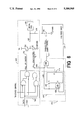
Images


Classifications
-
- H—ELECTRICITY
- H03—ELECTRONIC CIRCUITRY
- H03K—PULSE TECHNIQUE
- H03K19/00—Logic circuits, i.e. having at least two inputs acting on one output; Inverting circuits
- H03K19/003—Modifications for increasing the reliability for protection
- H03K19/00369—Modifications for compensating variations of temperature, supply voltage or other physical parameters
- H03K19/00384—Modifications for compensating variations of temperature, supply voltage or other physical parameters in field effect transistor circuits
-
- H—ELECTRICITY
- H03—ELECTRONIC CIRCUITRY
- H03K—PULSE TECHNIQUE
- H03K19/00—Logic circuits, i.e. having at least two inputs acting on one output; Inverting circuits
- H03K19/003—Modifications for increasing the reliability for protection
- H03K19/00346—Modifications for eliminating interference or parasitic voltages or currents
- H03K19/00361—Modifications for eliminating interference or parasitic voltages or currents in field effect transistor circuits
Definitions
- the present invention relates generally to communications between integrated circuits and more particularly to driver circuits which drive the communication lines between integrated circuits.
- Modern integrated circuits commonly come in the form of chips.
- the integrated circuits within a chip communicate with the world outside the chip through metalization layers on the outside of the chip known as signal pads.
- signal pads For communication from within the chip to the world outside, "driver circuits" drive signals or data through the signal pads on the exterior of the chip.
- the signal pads of various chips are connected together by signal lines thereby allowing communications between different chips.
- the signal pads on a chip are then connected to the packaging of the chip which is then connected to a transmission line on a printed circuit board which runs to another integrated circuit chip or other similar device.
- the electrical connection from the signal pad through the packaging of the chip to the transmission line contains parasitic inductance and capacitance which interferes with the transmission of the signal from the signal pad.
- the transmission line itself also contains transmission line characteristics which include capacitance and inductance which also interfere with the transmission of the signal from the signal pad. All of the foregoing add to the load which must be driven by the driver circuit.
- the driver circuits that drive those signal interconnections must be designed to avoid excessive voltage swings when switching occurs. Excessive voltage swings are known as ringing. Ringing must be avoided while still switching as fast as possible to meet the high speed performance requirements of modern integrated circuits.
- CMOS drivers have utilized NMOS (and/or PMOS) FET's to drive the signal pad to a voltage level based on a clocked or static input to the driver input.
- the drive NMOS FET's are turned on or off based on the inputs from inside the chip and stay in that state, regardless of the state of the transmission line being driven.
- a typical driver circuit as described above is shown in FIG. 1.
- the signal pad 102 in this case example is only used for driving signals out from the chip.
- FET 104 acts like an on/off switch and is controlled by line 106, labeled PULLUP CONTROL.
- line 106 When line 106 is in its high state (a digital 1) FET 104 acts like a switch turned on and pulls line 108, which drives signal pad 102, to voltage level Vdl (a digital 1 or "high") present at point 110.
- Vdl a digital 1 or "high
- the actual voltage attained by the signal pad is designated Voh. Voh may vary from Vdl due to, for example, leakage current from the device being driven by the signal pad 102.
- FET 112 is used to pull line 108 to ground 116 (0 volts).
- Line 114 labeled PULLDOWN CONTROL is applied to the gate of FET 112.
- FET 112 acts like a switch in the on position and line 108 is pulled towards ground (a digital 0 or "low”).
- the actual low voltage attained by the signal pad is designated Vol. Vol may be slightly higher than ground due to, for example, leakage current from the device being driven by the signal pad 102.
- Signal pad 102 can also be put into a tri-state mode which occurs when both line 106 and line 114 are at low logic levels and therefore both FET 104 and FET 112 act like switches in the off position and therefore line 108 is tri-stated. This could be used if pad 102 is also used to receive signals (input).
- the PULLUP CONTROL signal present on line 106 is a function of the signals TRI-STATE CONTROL, DATA TO BE DRIVEN, and CLOCK.
- the logical expression which defines the PULLUP CONTROL signal can be expressed as follows: ##STR1## (wherein the symbol "•" represents the logical AND function).
- That logical equation is implemented in the portion of the logic circuits 125 shown in FIG. 1 which generate the PULLUP CONTROL signal.
- the PULLDOWN CONTROL signal present on line 114 is also a function of the signals TRI-STATE CONTROL, DATA TO BE DRIVEN, and CLOCK.
- the logical expression which defines PULLDOWN CONTROL is as follows: ##STR2## (wherein the symbol "•" represents the logical AND function).
- FIG. 2 is a timing diagram showing the timing of the signals CLOCK and PULLDOWN CONTROL and the voltage present on the signal pad 102.
- FIG. 2 represents the slow case defined previously.
- the PULLDOWN CONTROL signal 204 goes high (a logical 1).
- FET 112 then operates as a switch in the on position and attempts to pull line 108 to ground.
- the voltage present on the signal pad represented by line 206 is then drawn down towards ground, to Vol.
- the irregularity 208 in line 206 is caused by reflection in the transmission line.
- the transition of the voltage present on signal pad 102 from Voh to Vol is relatively slow because of the high impedance of FET 112 in the slow case.
- the impedance of FET 112 would be high in the slow case because of high operating temperatures or due to process variations in the manufacturing of the chip.
- FIG. 3 is a timing diagram again showing the signals CLOCK and PULLDOWN CONTROL and the voltage present on the signal pad 102.
- FIG. 3 represents the "fast" case, also previously defined.
- the voltage of the PULLDOWN CONTROL signal represented by line 304 is at the high level.
- FET 112 again acts like a switch in the on position creating a connection from line 108 to ground 116.
- the voltage level on the signal pad represented in FIG. 3 by the line 306 is pulled to Vol.
- the irregularity 310 in the voltage present on the signal pad indicated by line 304 is caused by reflection of the transmission line connected to the signal pad.
- Undershoot (voltage below ground) 308 is caused by the parasitic inductance and capacitance in the connections from the signal pad to the transmission line and to a lesser degree from the characteristics of the transmission line being driven by the signal pad. Bounce 311 is a result of the undershoot 308 and can cause communication errors.
- the present invention is an output driver for an integrated circuit.
- the present invention varies the impedance of the driver circuit based upon the output voltage level present on the output pad. Therefore, the output drive partially compensates for process variations and interconnect parasitic.
- this is accomplished by using two smaller FET's to pull the voltage of the driver output pad.
- One of the smaller FET's is controlled in the same manner as the single FET is controlled in earlier designs. That FET is simply turned on when the output is to be driven low and stays on.
- the other smaller FET is used to vary total impedance of the driver by using feedback from the signal pad to sense when pad voltage has reached a threshold level and to then turn off the second driver FET.
- FIG. 1 is a schematic diagram of a prior art driver circuit.
- FIG. 2 is a timing diagram for the "slow" case for the circuit of FIG. 1.
- FIG. 3 is a timing diagram of the "fast" case for the circuit of FIG. 1.
- FIG. 4 is a block diagram of a preferred embodiment of the present invention and its operating environment.
- FIG. 5 is a block diagram of a preferred embodiment of the present invention.
- FIG. 6 is a schematic diagram of a preferred embodiment of the present invention.
- FIG. 7 is a timing diagram of the slow case for the circuit of FIG. 6.
- FIG. 8 is a timing diagram of the fast case for the circuit of FIG. 6.
- FIG. 9 is a flow diagram of the operation of a preferred embodiment of the present invention.
- FIG. 4 is a block diagram of an integrated circuit 402 which contains a preferred embodiment of the present invention.
- the box labeled CHIP LOGIC 404 indicates the circuitry of integrated circuit 402 excluding the driver circuit 406 and the signal pad 408.
- the signal pad 408 is connected to transmission line 410 via the packaging connection 412.
- the box labeled 414 represents the parasitic capacitance and inductance of the packaging connection 412 and any associated resistance.
- the box labeled 416 represents the characteristics of the transmission line 410.
- Transmission line 410 provides a signal path to the input of another integrated circuit or similar device to which integrated circuit 402 sends data.
- Driver circuit 406 receives inputs from chip logic 404.
- the inputs preferably include a clock signal and data to be transmitted or driven to pad 408.
- Chip logic 404 may also supply a tri-state signal to driver circuit 406.
- Driver circuit 406 drives a signal via line 418 through signal pad 408.
- the driver circuit receives a feedback signal over line 420 from signal pad 408.
- FIG. 5 shows a preferred embodiment of the driver circuit, the signal pad and the associated interconnections in more detail.
- the control logic 502 receives the signals TRI-STATE CONTROL, DATA TO BE DRIVEN, and CLOCK from the chip logic 404 shown in FIG. 4.
- the control logic 502 contains the logical circuit in the dashed box 125 in FIG. 1.
- control logic 502 could be implemented in various other ways and perform additional or different functions without departing from the scope and spirit of the present invention.
- control logic 502 could be edge triggered, could operate as a static driver (operating without a clock), and/or could incorporate a multiplexer for multiplexing data.
- Control logic 502 could also receive and respond to inputs other than those shown and still operate within the scope of the present invention.
- control logic 502 implements the logic table shown below.
- a signal PULL UP CONTROL (labeled “PULL UP" in the logic table above) is connected to the gate of FET 504.
- FET 504 When signal PULL UP CONTROL is high (a logical 1) FET 504 operates like a switch in the on position and connects the signal pad to the voltage level Vdl.
- signal PULL UP CONTROL When signal PULL UP CONTROL is low (a logical 0) FET 504 operates like a switch in the off position and disconnects signal pad 408 from Vdl.
- a signal PULL DOWN CONTROL (labeled “PULL DOWN" in the logic table above) is attached to the gate of FET 512.
- PULL DOWN CONTROL When the signal pull down control is high (a logical 1), FET 512 operates like a switch in the on position and connects signal pad 408 to ground.
- the signal PULL DOWN CONTROL When the signal PULL DOWN CONTROL is low (a logical 0), FET 512 operates like a switch in the off position and disconnects signal pad 408 from ground.
- a signal VARIABLE PULL DOWN CONTROL is connected to the gate of FET 518.
- FET 518 acts like a switch in the on position and connects signal pad 408 to ground.
- VARIABLE PULL DOWN CONTROL is low (a logical 0)
- FET 518 operates like a switch in the off position and signal pad 408 sees a high impedance.
- the feedback logic 503 generates the VARIABLE PULL DOWN CONTROL signal.
- the signal VARIABLE PULL DOWN CONTROL is a function of the signal PULL DOWN CONTROL and the feedback from the signal pad carried along line 420.
- FIG. 6 A preferred embodiment of the circuit depicted in FIG. 5 will now be discussed with reference to FIG. 6.
- the portion of the circuit located within the dashed box 602 is nearly identical to the circuit depicted in FIG. 1.
- the portion of the circuit within box 602 has therefor been previously described and will only be described again where necessary.
- the signal pad 408 in this exemplary embodiment is only used for driving signals out from the chip.
- the circuit of FIG. 6 could easily be modified for use for both input and output, or could be logically implemented many other ways to achieve the same function.
- the circuit within dashed box 503 includes a latch circuit 613.
- Line 606 carries the PULLDOWN CONTROL signal from line 114 to AND gate 608.
- the PULLDOWN CONTROL signal is also carried by line 610 to an inverter 612 located at the S (set) input of flipflop 614 and to an input of AND gate 616.
- Flipflop 614 is a standard level driven SRQ flip and will go to a high output (digital logic 1) at its Q output whenever a high level occurs at its S input. The output at its Q output will go to a low level (digital logic) whenever a high level occurs at its R (reset) input.
- a FET 518 is electrically connected to line 108 via line 620. The other end of FET 518 is connected to ground.
- Line 622 labeled VARIABLE PULLDOWN CONTROL is connected to the gate of FET 518. Therefore, when line 622 is in its "high" state (a digital logic 1), FET 518 acts like a switch in the on position and line 620 is connected directly to ground.
- the PAD FEEDBACK line 420 provides a feedback signal from line 620 to an inverter 626 located at an input to AND gate 616. The output from AND gate 616 is connected to the R input (the reset) of flipflop 614.
- FIG. 6 The section of FIG. 6 in dashed box 602 functions in much the same way as the circuit in FIG. 1.
- FET 512 acts like a switch in the on position connecting line 108 to ground.
- Line 606 also provides a high input to AND gate 608 and line 610 provides a high input to the inverter 612 and to an input of AND gate 616.
- FIG. 7 shows a timing diagram of the signals CLOCK, PULLDOWN CONTROL and VARIABLE PULLDOWN CONTROL and the voltage present on the signal pad (SIGNAL PAD) in the slow case which was defined in the RELATED ART section of this document.
- the Q output of flipflop 614 is initially high (a logical 1). That is a result of the signal PULLDOWN CONTROL having initially been a low value when the CLOCK was low.
- the signal PULLDOWN CONTROL goes high (a logical 1), when data is low (a logical one).
- FET 512 acts like a switch in the on position and begins pulling the voltage of the signal pad 408 towards ground, to Vol.
- the PULLDOWN CONTROL signal reaches its high value, the inputs to AND gate 608 are both high. Therefore, the signal VARIABLE PULLDOWN CONTROL would go high.
- the signal VARIABLE PULLDOWN CONTROL (on line 622) controls FET 518. Therefore, when the signal VARIABLE PULLDOWN CONTROL is high, FET 518 acts like a switch in the on position and also begins pulling signal pad 408 down to voltage level Vol. Therefore, both FET's 512 and 518 act in parallel to pull signal pad 408 down towards ground, to voltage level Vol. Because FET 512 and FET 518 act in parallel, the resistance between signal pad 408 and ground is one half what it would be if a single FET was used.
- the time interval indicated in FIG. 7 as 704 is the propagation delay from the time the signal pad reaches the level Vth to the time the signal VARIABLE PULLDOWN CONTROL leaves its high state and turns 518 "off".
- Time interval 704 is due to the propagation delay within the feedback logic 503. In the slow case, that delay is a significant amount of time.
- FIG. 8 is a timing diagram for the circuit of FIG. 6 in the fast case.
- the transition of the signal pad from a high level to a low level in the fast case will now be described with reference to FIGS. 6, 8 and 9.
- the Q output of flipflop 614 is initially high (a logical 1).
- the PULLDOWN CONTROL signal is at a high level (a logical 1) (box 902 of FIG. 9).
- FET 512 acts like a switch in the on position (box 904 of FIG. 9) and begins pulling the voltage of signal pad 408 down towards ground to voltage Vol.
- AND gate 608 sees the high level of the PULLDOWN CONTROL signal at one of its inputs and the high level from the output of flipflop 614 at its other input and therefore outputs a high level along 622, the VARIABLE PULLDOWN CONTROL signal (box 906 of FIG. 9).
- the VARIABLE PULLDOWN CONTROL signal reaches its high state, it turns FET 518 on (box 908 of FIG. 9), and FET 518 also begins pulling the voltage on signal pad 408 down towards ground.
- inverter 626 When the voltage present at the pad 408, fed back to inverter 622 via PAD FEEDBACK 420, reaches the level indicated the threshold level for inverter 626, Vth (box 910 in FIG. 9), inverter 626 outputs a high level to AND gate 616 which is also receiving a high level from the PULLDOWN CONTROL signal via lines 606 and 610. AND gate 616 then outputs a high level to the R(reset) input of flipflop 614 which causes the flipflop to reset and output a low level at its Q output. The low level output by flipflop 614 is input to AND gate 608 which then outputs a low level along line 622, the VARIABLE PULLDOWN CONTROL signal (box 912 of FIG. 9). The low level on line 622 turns FET 518 off (box 914 of FIG. 9). The interval during which FET 518 is "on” is labeled "on” in FIG. 8.
- the FET 512 operating along has a larger resistance than the two FET's operating together or the single FET 112 of the previous design and, therefore, the voltage present on pad 408 falls less steeply which decreases the ringing caused by the voltage transition compared to prior circuits.
- the timing of the circuit can be adjusted by adjusting Vth which is most easily accomplished in the circuit depicted in FIG. 6 by varying the channel lengths of the FET' s used to implement inverter 626.
- FIGS. 4-6 can also be applied to the pullup control 106. Further, the particular logic circuits depicted in the control logic block 502 and the feedback control block 503 could easily be varied to equivalent logical circuits without departing from the spirit and scope of this invention.
- the present invention is an output driver for an integrated circuit which compensates for process variations in environmental factors which alter the impedance of the circuit.
- the present invention varies the impedance of the driver circuit based upon the output voltage level present on the output pad. Therefore, the output driver circuit of the present invention compensates for process variations and interconnect parasitics. While preferred embodiments of the present invention have been set forth, various modifications, alterations and changes may be made without the parting from the spirit and scope of the present invention as defined in the following claims.
Abstract
Description
______________________________________
INPUTS             OUTPUTS
Tri-State Data   Clock     Pull Up
                                  Pull Down
______________________________________
0         0      0         0      0
0         0      1         0      1
0         1      0         0      0
0         1      1         1      0
1         0      0         0      0
1         0      1         0      0
1         1      0         0      0
1         1      1         0      0
______________________________________
Claims (13)
Priority Applications (1)
| Application Number | Priority Date | Filing Date | Title |
|---|---|---|---|
| US07/907,362 US5306965A (en) | 1992-07-01 | 1992-07-01 | Process compensating variable impedence I/O driver with feedback |
Applications Claiming Priority (1)
| Application Number | Priority Date | Filing Date | Title |
|---|---|---|---|
| US07/907,362 US5306965A (en) | 1992-07-01 | 1992-07-01 | Process compensating variable impedence I/O driver with feedback |
Publications (1)
| Publication Number | Publication Date |
|---|---|
| US5306965A true US5306965A (en) | 1994-04-26 |
Family
ID=25423959
Family Applications (1)
| Application Number | Title | Priority Date | Filing Date |
|---|---|---|---|
| US07/907,362 Expired - Lifetime US5306965A (en) | 1992-07-01 | 1992-07-01 | Process compensating variable impedence I/O driver with feedback |
Country Status (1)
| Country | Link |
|---|---|
| US (1) | US5306965A (en) |
Cited By (24)
| Publication number | Priority date | Publication date | Assignee | Title |
|---|---|---|---|---|
| US5442304A (en) * | 1993-10-15 | 1995-08-15 | Advanced Micro Devices, Inc. | CMOS logic gate clamping circuit |
| US5481208A (en) * | 1993-10-28 | 1996-01-02 | United Microelectronics Corp. | Piecewisely-controlled tri-state output buffer |
| US5500817A (en) * | 1993-01-21 | 1996-03-19 | Micron Technology, Inc. | True tristate output buffer and a method for driving a potential of an output pad to three distinct conditions |
| US5546039A (en) * | 1994-11-02 | 1996-08-13 | Advanced Micro Devices, Inc. | Charge dissipation in capacitively loaded ports |
| US5568062A (en) * | 1995-07-14 | 1996-10-22 | Kaplinsky; Cecil H. | Low noise tri-state output buffer |
| US5675270A (en) * | 1996-01-30 | 1997-10-07 | Xilinx, Inc. | Data line with dynamic pull-up circuit |
| US5698994A (en) * | 1994-07-29 | 1997-12-16 | Nkk Corporation | Data output circuit, intermediate potential setting circuit, and semiconductor integrated circuit |
| US5731738A (en) * | 1992-07-21 | 1998-03-24 | Advanced Micro Devices, Inc. | Method and mechanism of weak pull-up for use with a microcontroller in an integrated circuit |
| US5831908A (en) * | 1994-07-29 | 1998-11-03 | Nkk Corporation | Data output circuit, intermediate potential setting circuit, and semiconductor integrated circuit |
| US5869983A (en) * | 1997-03-24 | 1999-02-09 | Intel Corporation | Method and apparatus for controlling compensated buffers |
| US5952850A (en) * | 1996-09-25 | 1999-09-14 | Kabushiki Kaisha Toshiba | Input/output circuit and a method for controlling an input/output signal |
| US5959481A (en) * | 1997-02-18 | 1999-09-28 | Rambus Inc. | Bus driver circuit including a slew rate indicator circuit having a one shot circuit |
| US6060921A (en) * | 1997-09-29 | 2000-05-09 | Cypress Semiconductor Corp. | Voltage threshold detection circuit |
| US6100727A (en) * | 1998-02-03 | 2000-08-08 | Nec Corporation | Noise-immune dynamic driving circuit capable of suppressing generation of a feedthrough current and increase of a delay |
| US6118310A (en) * | 1998-11-04 | 2000-09-12 | Agilent Technologies | Digitally controlled output driver and method for impedance matching |
| US6208185B1 (en) * | 1999-03-25 | 2001-03-27 | Wisconsin Alumni Research Corporation | High performance active gate drive for IGBTs |
| US6222397B1 (en) * | 1997-09-18 | 2001-04-24 | Oki Electric Industry Co., Ltd. | Output circuit with switching function |
| US6229845B1 (en) * | 1999-02-25 | 2001-05-08 | Qlogic Corporation | Bus driver with data dependent drive strength control logic |
| US6239617B1 (en) * | 1999-11-04 | 2001-05-29 | International Business Machines Corporation | Mixed voltage output driver with automatic impedance adjustment |
| US6265914B1 (en) * | 1999-11-19 | 2001-07-24 | Lsi Logic Corporation | Predriver for high frequency data transceiver |
| US6407594B1 (en) * | 1993-04-09 | 2002-06-18 | Sgs-Thomson Microelectronics S.R.L. | Zero bias current driver control circuit |
| US6760380B1 (en) | 1998-12-07 | 2004-07-06 | Lynk Labs, Inc. | Data transmission apparatus and method |
| US20080065820A1 (en) * | 1998-07-27 | 2008-03-13 | Peter Gillingham | High bandwidth memory interface |
| US20130002327A1 (en) * | 2011-06-28 | 2013-01-03 | Texas Instruments, Incorporated | Bias temperature instability-resistant circuits |
Citations (6)
| Publication number | Priority date | Publication date | Assignee | Title |
|---|---|---|---|---|
| US4777389A (en) * | 1987-08-13 | 1988-10-11 | Advanced Micro Devices, Inc. | Output buffer circuits for reducing ground bounce noise |
| US4779013A (en) * | 1985-08-14 | 1988-10-18 | Kabushiki Kaisha Toshiba | Slew-rate limited output driver having reduced switching noise |
| US4880997A (en) * | 1988-08-18 | 1989-11-14 | Ncr Corporation | Low noise output buffer circuit |
| US5015880A (en) * | 1989-10-10 | 1991-05-14 | International Business Machines Corporation | CMOS driver circuit |
| US5091658A (en) * | 1988-11-17 | 1992-02-25 | Siemens Aktiengesellschaft | Circuit configuration for noise signal compensation |
| US5153457A (en) * | 1990-12-12 | 1992-10-06 | Texas Instruments Incorporated | Output buffer with di/dt and dv/dt and tri-state control |
-
1992
- 1992-07-01 US US07/907,362 patent/US5306965A/en not_active Expired - Lifetime
Patent Citations (6)
| Publication number | Priority date | Publication date | Assignee | Title |
|---|---|---|---|---|
| US4779013A (en) * | 1985-08-14 | 1988-10-18 | Kabushiki Kaisha Toshiba | Slew-rate limited output driver having reduced switching noise |
| US4777389A (en) * | 1987-08-13 | 1988-10-11 | Advanced Micro Devices, Inc. | Output buffer circuits for reducing ground bounce noise |
| US4880997A (en) * | 1988-08-18 | 1989-11-14 | Ncr Corporation | Low noise output buffer circuit |
| US5091658A (en) * | 1988-11-17 | 1992-02-25 | Siemens Aktiengesellschaft | Circuit configuration for noise signal compensation |
| US5015880A (en) * | 1989-10-10 | 1991-05-14 | International Business Machines Corporation | CMOS driver circuit |
| US5153457A (en) * | 1990-12-12 | 1992-10-06 | Texas Instruments Incorporated | Output buffer with di/dt and dv/dt and tri-state control |
Cited By (33)
| Publication number | Priority date | Publication date | Assignee | Title |
|---|---|---|---|---|
| US5731738A (en) * | 1992-07-21 | 1998-03-24 | Advanced Micro Devices, Inc. | Method and mechanism of weak pull-up for use with a microcontroller in an integrated circuit |
| US5500817A (en) * | 1993-01-21 | 1996-03-19 | Micron Technology, Inc. | True tristate output buffer and a method for driving a potential of an output pad to three distinct conditions |
| US6407594B1 (en) * | 1993-04-09 | 2002-06-18 | Sgs-Thomson Microelectronics S.R.L. | Zero bias current driver control circuit |
| US5442304A (en) * | 1993-10-15 | 1995-08-15 | Advanced Micro Devices, Inc. | CMOS logic gate clamping circuit |
| US5481208A (en) * | 1993-10-28 | 1996-01-02 | United Microelectronics Corp. | Piecewisely-controlled tri-state output buffer |
| US5831908A (en) * | 1994-07-29 | 1998-11-03 | Nkk Corporation | Data output circuit, intermediate potential setting circuit, and semiconductor integrated circuit |
| US5698994A (en) * | 1994-07-29 | 1997-12-16 | Nkk Corporation | Data output circuit, intermediate potential setting circuit, and semiconductor integrated circuit |
| US5546039A (en) * | 1994-11-02 | 1996-08-13 | Advanced Micro Devices, Inc. | Charge dissipation in capacitively loaded ports |
| US5568062A (en) * | 1995-07-14 | 1996-10-22 | Kaplinsky; Cecil H. | Low noise tri-state output buffer |
| US5675270A (en) * | 1996-01-30 | 1997-10-07 | Xilinx, Inc. | Data line with dynamic pull-up circuit |
| US5952850A (en) * | 1996-09-25 | 1999-09-14 | Kabushiki Kaisha Toshiba | Input/output circuit and a method for controlling an input/output signal |
| US5959481A (en) * | 1997-02-18 | 1999-09-28 | Rambus Inc. | Bus driver circuit including a slew rate indicator circuit having a one shot circuit |
| US5869983A (en) * | 1997-03-24 | 1999-02-09 | Intel Corporation | Method and apparatus for controlling compensated buffers |
| US6222397B1 (en) * | 1997-09-18 | 2001-04-24 | Oki Electric Industry Co., Ltd. | Output circuit with switching function |
| US6384644B2 (en) * | 1997-09-18 | 2002-05-07 | Oki Electric Industry Co, Ltd. | Output circuit with switching function |
| US6060921A (en) * | 1997-09-29 | 2000-05-09 | Cypress Semiconductor Corp. | Voltage threshold detection circuit |
| US6100727A (en) * | 1998-02-03 | 2000-08-08 | Nec Corporation | Noise-immune dynamic driving circuit capable of suppressing generation of a feedthrough current and increase of a delay |
| US7765376B2 (en) | 1998-07-27 | 2010-07-27 | Mosaid Technologies Incorporated | Apparatuses for synchronous transfer of information |
| US8654573B2 (en) | 1998-07-27 | 2014-02-18 | Mosaid Technologies Incorporated | High bandwidth memory interface |
| US8266372B2 (en) | 1998-07-27 | 2012-09-11 | Mosaid Technologies Incorporated | High bandwidth memory interface |
| US8250297B2 (en) | 1998-07-27 | 2012-08-21 | Mosaid Technologies Incorporated | High bandwidth memory interface |
| US20100268906A1 (en) * | 1998-07-27 | 2010-10-21 | Mosaid Technologies Incorporated | High bandwidth memory interface |
| US20080065820A1 (en) * | 1998-07-27 | 2008-03-13 | Peter Gillingham | High bandwidth memory interface |
| US20080120458A1 (en) * | 1998-07-27 | 2008-05-22 | Peter Gillingham | High bandwidth memory interface |
| US20080120457A1 (en) * | 1998-07-27 | 2008-05-22 | Mosaid Technologies Incorporated | Apparatuses for synchronous transfer of information |
| US6118310A (en) * | 1998-11-04 | 2000-09-12 | Agilent Technologies | Digitally controlled output driver and method for impedance matching |
| US6760380B1 (en) | 1998-12-07 | 2004-07-06 | Lynk Labs, Inc. | Data transmission apparatus and method |
| US6229845B1 (en) * | 1999-02-25 | 2001-05-08 | Qlogic Corporation | Bus driver with data dependent drive strength control logic |
| US6208185B1 (en) * | 1999-03-25 | 2001-03-27 | Wisconsin Alumni Research Corporation | High performance active gate drive for IGBTs |
| US6239617B1 (en) * | 1999-11-04 | 2001-05-29 | International Business Machines Corporation | Mixed voltage output driver with automatic impedance adjustment |
| US6265914B1 (en) * | 1999-11-19 | 2001-07-24 | Lsi Logic Corporation | Predriver for high frequency data transceiver |
| US20130002327A1 (en) * | 2011-06-28 | 2013-01-03 | Texas Instruments, Incorporated | Bias temperature instability-resistant circuits |
| US8786307B2 (en) * | 2011-06-28 | 2014-07-22 | Texas Instruments Incorporated | Bias temperature instability-resistant circuits |
Similar Documents
| Publication | Publication Date | Title |
|---|---|---|
| US5306965A (en) | Process compensating variable impedence I/O driver with feedback | |
| US5877647A (en) | CMOS output buffer with slew rate control | |
| US5568062A (en) | Low noise tri-state output buffer | |
| US6424170B1 (en) | Apparatus and method for linear on-die termination in an open drain bus architecture system | |
| US6759868B2 (en) | Circuit and method for compensation if high-frequency signal loss on a transmission line | |
| EP0493873B1 (en) | CMOS output buffer circuit with ground bounce reduction | |
| US5347177A (en) | System for interconnecting VLSI circuits with transmission line characteristics | |
| US5497105A (en) | Programmable output pad with circuitry for reducing ground bounce noise and power supply noise and method therefor | |
| US5717343A (en) | High-drive CMOS output buffer with noise supression using pulsed drivers and neighbor-sensing | |
| US6255867B1 (en) | CMOS output buffer with feedback control on sources of pre-driver stage | |
| US5367210A (en) | Output buffer with reduced noise | |
| JP2000091904A (en) | Cmos buffer having constant impedance with low noise | |
| WO1996001009A9 (en) | A noise-reducing programmable output circuit | |
| US5097148A (en) | Integrated circuit buffer with improved drive capability | |
| US6459325B1 (en) | Output buffer having a pre-driver transition controller | |
| US6559676B1 (en) | Output buffer circuit | |
| US6278306B1 (en) | Method for an output driver with improved slew rate control | |
| US6366139B1 (en) | Method for an output driver with improved impedance control | |
| US6448807B1 (en) | Dynamic impedance controlled driver for improved slew rate and glitch termination | |
| US6356102B1 (en) | Integrated circuit output buffers having control circuits therein that utilize output signal feedback to control pull-up and pull-down time intervals | |
| US6060938A (en) | Output buffer for reducing switching noise | |
| US5917335A (en) | Output voltage controlled impedance output buffer | |
| US6359465B1 (en) | CMOS small signal switchable adjustable impedence terminator network | |
| US7276939B2 (en) | Semiconductor integrated circuit | |
| KR100342210B1 (en) | Transceiver driver with programmable edge rate control independent of fabrication process, supply voltage, and temperature |
Legal Events
| Date | Code | Title | Description |
|---|---|---|---|
| AS | Assignment |
Owner name: HEWLETT-PACKARD COMPANY, CALIFORNIA Free format text: ASSIGNMENT OF ASSIGNORS INTEREST.;ASSIGNOR:ASPREY, THOMAS A.;REEL/FRAME:006387/0153 Effective date: 19920811 |
|
| STCF | Information on status: patent grant |
Free format text: PATENTED CASE |
|
| FEPP | Fee payment procedure |
Free format text: PAYOR NUMBER ASSIGNED (ORIGINAL EVENT CODE: ASPN); ENTITY STATUS OF PATENT OWNER: LARGE ENTITY |
|
| FPAY | Fee payment |
Year of fee payment: 4 |
|
| AS | Assignment |
Owner name: HEWLETT-PACKARD COMPANY, COLORADO Free format text: MERGER;ASSIGNOR:HEWLETT-PACKARD COMPANY;REEL/FRAME:011523/0469 Effective date: 19980520 |
|
| FPAY | Fee payment |
Year of fee payment: 8 |
|
| FPAY | Fee payment |
Year of fee payment: 12 |