US5519847A - Method of pipelining sequential writes in a flash memory - Google Patents
Method of pipelining sequential writes in a flash memory Download PDFInfo
- Publication number
- US5519847A US5519847A US08/085,969 US8596993A US5519847A US 5519847 A US5519847 A US 5519847A US 8596993 A US8596993 A US 8596993A US 5519847 A US5519847 A US 5519847A
- Authority
- US
- United States
- Prior art keywords
- plane
- flash memory
- page buffer
- data
- memory device
- Prior art date
- Legal status (The legal status is an assumption and is not a legal conclusion. Google has not performed a legal analysis and makes no representation as to the accuracy of the status listed.)
- Expired - Lifetime
Links
- 238000000034 method Methods 0.000 title claims abstract description 46
- 239000000872 buffer Substances 0.000 claims abstract description 132
- 230000011664 signaling Effects 0.000 claims description 5
- 230000003068 static effect Effects 0.000 claims description 5
- 230000008878 coupling Effects 0.000 claims 11
- 238000010168 coupling process Methods 0.000 claims 11
- 238000005859 coupling reaction Methods 0.000 claims 11
- 238000012546 transfer Methods 0.000 description 16
- 238000010586 diagram Methods 0.000 description 9
- 230000008520 organization Effects 0.000 description 6
- 238000013500 data storage Methods 0.000 description 3
- 230000008901 benefit Effects 0.000 description 2
- 230000006870 function Effects 0.000 description 2
- 230000008569 process Effects 0.000 description 2
- 238000012545 processing Methods 0.000 description 2
- 230000003139 buffering effect Effects 0.000 description 1
- 230000001351 cycling effect Effects 0.000 description 1
- 230000007423 decrease Effects 0.000 description 1
- 230000003247 decreasing effect Effects 0.000 description 1
- 230000000977 initiatory effect Effects 0.000 description 1
- 238000012986 modification Methods 0.000 description 1
- 230000004048 modification Effects 0.000 description 1
- 230000004044 response Effects 0.000 description 1
- 238000012163 sequencing technique Methods 0.000 description 1
- 238000012360 testing method Methods 0.000 description 1
Images


Classifications
-
- G—PHYSICS
- G11—INFORMATION STORAGE
- G11C—STATIC STORES
- G11C16/00—Erasable programmable read-only memories
- G11C16/02—Erasable programmable read-only memories electrically programmable
- G11C16/06—Auxiliary circuits, e.g. for writing into memory
- G11C16/10—Programming or data input circuits
-
- G—PHYSICS
- G11—INFORMATION STORAGE
- G11C—STATIC STORES
- G11C7/00—Arrangements for writing information into, or reading information out from, a digital store
- G11C7/10—Input/output [I/O] data interface arrangements, e.g. I/O data control circuits, I/O data buffers
- G11C7/1015—Read-write modes for single port memories, i.e. having either a random port or a serial port
- G11C7/1039—Read-write modes for single port memories, i.e. having either a random port or a serial port using pipelining techniques, i.e. using latches between functional memory parts, e.g. row/column decoders, I/O buffers, sense amplifiers
Definitions
- the present invention pertains to flash memory devices. More particularly, this invention relates to a method of increasing the data throughput of a flash memory device including a page buffer having two planes.
- Typical flash memory devices contain a nonvolatile memory cell array for random access data storage. Some prior flash memory devices also include a write control circuit for programming and erasing the memory cell array.
- Prior flash memory devices may employ an on-chip data buffer to increase programming throughput of the flash cell array.
- the data buffer enables increased programming speed by buffering programming data.
- the data buffer enables fast access to the programming data by the write control circuit.
- the fast access to the programming data enables the write control circuit to amortize the cycling of program level voltages across multiple bytes in the flash cell array.
- a user typically provides an input/output driver that loads programming data into the data buffer.
- the input/output driver then issues a program command to the write control circuit. Thereafter, the write control circuit accesses the data within the data buffer and uses that data to program the flash cell array.
- the input/output driver can load another block of data into the data buffer only after the write control circuit completes programming, and is no longer accessing the data buffer.
- the input/output driver idles while waiting for the write control circuit to complete the program operation.
- the idle time of the input/output driver reduces programming throughput and data throughput of the flash memory device.
- An object of the present invention is to improve the data throughput of a flash memory device by using a page buffer within the flash memory device.
- a method of increasing the data throughput of a memory device including a page buffer is described.
- Data throughput is increased by pipelining write operations such that one plane of the page buffer is being used to program the memory array of the memory device while the other plane of the page buffer is being loaded by an external user with data to be used in the next program operation.
- the first write operation is set up by loading a first block of data into the first plane of the page buffer.
- the first operation begins with the external user commanding the memory device to program the memory array with the first block of data stored in the first plane.
- the second write operation is setup by the external user immediately following the first command to program.
- the second write operation is setup by loading a second block of data into the second plane of the page buffer while the memory array is being programmed from the first plane.
- the second write operation begins with the external user commanding the array controller to program the flash memory array with the second block of data stored in the second plane.
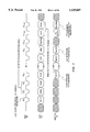
- FIG. 1 is a block diagram of a computer system.
- FIG. 2 is a block diagram of a flash memory device.
- FIG. 3 is a block diagram of the page buffer.
- FIG. 4 illustrates the architecture of Plane A and Plane B of the plane buffer.
- FIG. 5 describes the modes of the page buffer.
- FIG. 6 illustrates a method of pipelining writes to a flash memory device.
- FIG. 7 illustrates the control, address and data signals for a write cycle using the method of FIG. 6.
- FIG. 8 illustrates the interleaving of program operations using the page buffer.
- FIG. 9 is a block diagram of the interface circuit.
- FIG. 10 illustrates the address bit fields for accessing the page buffer.
- FIG. 11 illustrates plane assignment of the page buffer for accesses by the flash array controller.
- FIG. 12 illustrates plane assignment of the page buffer for accesses by the interface circuit.
- FIG. 13 is a truth table of the states of plane B select signals.
- FIG. 14 is a truth table of the states of the plane A select signals.
- FIG. 15 is a block diagram of the output data aligner circuit.
- FIG. 16 is a truth table for the output data aligner circuit.
- FIG. 17 is another truth table for the output data aligner circuit.
- FIG. 1 is a block diagram of computer system 300.
- Computer system 300 includes central processing unit (CPU) 302, main memory 304, and flash memory devices 310-314.
- CPU 302 communicates with main memory 304 and flash memory devices 310-314 over user bus 306.
- flash memory devices 310-314 provide random access, nonvolatile, large scale data storage.
- CPU 302 is able to eliminate dead time associated with performing sequential writes to random access memory and increase the data throughput of flash memory devices 310-314 using the method of the present invention.
- the method of performing sequential writes takes advantage of page buffer 70 within each flash memory chip 310, 312, and 314.
- CPU 302 is able to write, or load, data associated with one write command into page buffer 70 while write data associated with a previous write command is being written from page buffer 70 into the flash memory cell array of a flash memory device.
- FIG. 2 is a block diagram of the internal organization of flash memory device 310. Flash memory devices 312 and 314 are organized in the same fashion, and it will be understood that the discussion of flash memory device 310 applies equally to flash memory device 312 and 314. Flash memory device 310 includes flash memory cell array 20, interface circuit 40, flash array controller 50, page buffer 70, a set of control registers 80-83, and read/write path 30. External users, such as CPU 302, communicate with flash memory device 310 via user bus 306.
- User bus 306 includes user address bus 102, user data bus 104, and user control bus 106. These buses 102, 104 and 106 are appropriately coupled to pads, or pins, of flash memory device 310.
- Page buffer 70 is an array of static random access memory cells (SRAM), which serves multiple purposes within flash memory device 310. Page buffer 70 can be accessed both by CPU 302 and flash array controller 50. As will be described in more detail below, the organization of page buffer 70 permits CPU 302 to write to page buffer 70 while flash array controller 50 is also using page buffer 70 to program flash memory cell array 20.
- SRAM static random access memory cells
- Flash memory cell array 20 is an array of flash memory cells, which store data. In one embodiment, flash memory cell array 20 is organized as 32 blocks. Each block provides 64k bytes of data storage. In one embodiment, each block is 16 bits wide, but may be accessed by CPU 302 either by 8 bits or by 16 bits.
- Read/write path 30 includes read and write path circuitry for accessing flash memory cell array 20.
- Read/write path 30 includes row and column address decoding circuitry for decoding address signals and generating appropriate block select row and column signals for flash memory cell array 20.
- Read/write path 30 also includes a small array of reference flash cells, and sense path circuitry for comparing the reference flash cells to cells from flash memory cells array 20 to determine whether memory bits or cells store a logic 1 or logic 0.
- Control registers 80-83 contain specialized control registers and associated circuitry for controlling read/write path 30.
- the specialized control registers are programmed and accessed over central control bus 100.
- Control access circuit 60 enables both interface circuit 40 and flash array controller 50 to access control registers 80-83 over central control bus 100.
- Interface circuit 40 enables access to flash memory cell array 20 by receiving and processing commands received over user bus 306.
- Interface circuit 40 receives commands over user data bus 104, verifies the commands, and queues the commands to flash array controller 50 over queue bus 41. Thereafter, flash array controller 50 executes the command.
- Interface circuit 40 controls the selection of an input address 36 coupled to read/write path 30 via input address multiplexer 35.
- the selected input address 36 is either the address sensed by TTL buffers (not shown) on user address bus 102, or a latched address 37 from interface circuit 40.
- the input address 36 may be overridden by programming control registers of control register 84.
- Interface circuit 40 selects the source of output data to be coupled to user data bus 104. Interface circuit 40 does so by controlling controls output data multiplexer 45.
- the selected output data is either flash array data 46 from read/write path 30, page buffer data 47 from page buffer 70, or block status register (BSR) data 48 from a set of block status registers contained within interface circuit 40.
- BSR block status register
- Flash array controller 50 is a specialized processor for performing write operations on flash memory cell array 20. Flash array controller 50 uses the commands received over queue bus 41 to locate the appropriate instruction within a control store.
- CPU 302 reads flash memory cell array 20 by transferring address signals over user address bus 102 while signaling a read command over user control bus 106.
- Interface circuit 40 detects the read cycles and causes the input address multiplexer 35 to transfer the address signals on user address bus 102 through to the x and y decode circuitry of read/write path 30.
- Interface circuit 40 also causes the output data multiplexer 45 to transfer the addressed read data from the read/write path 30 over user data bus 104.
- CPU 302 writes data to flash memory cell array 20 by signaling a write command and using user bus 306 to transfer blocks of data to be programmed into page buffer 70.
- Interface circuit 40 verifies the write command, and queues the write command to flash array controller 50.
- Flash array controller 50 executes the write command by reading the data to be programmed from page buffer over controller bus 51, and by programming the appropriate address locations within flash memory cell array 20.
- Flash array controller 50 implements algorithms for sequencing the high voltage circuitry of read/write path 30 to program flash memory cell array 20 by applying charge to flash cells and to erase flash memory cell array 20 by removing charge from the flash cells. Flash array controller 50 controls the high voltage circuitry and addresses flash memory cell array 20 by accessing control registers 80-83 via central control bus 100.
- Read/write path 30 includes source switch circuitry for applying the appropriate voltage levels to flash memory cell array 20 for an erase function.
- Read/write path 30 also includes program load circuitry for driving program level voltages onto bit lines of flash memory cell array 20 during programming operations.
- Interface circuit 40 includes a global status register which indicates the status of page buffer 70. Flash array controller 50 maintains the status bits of the global status register.
- CPU 302 reads the contents of the global status registers via user bus 306.
- FIG. 3 is a block diagram illustrating page buffer 70.
- Page buffer 70 includes two 256 by 8 bit static random access memory (SRAM) planes, plane A and plane B.
- FIG. 4 illustrates the organization of Plane A 310 and Plane B 320 of page buffer 70. Plane A 310 and Plane B 320 each include two 128 ⁇ 8 bit columns, which are called column A and column B, respectively.
- Command bus 220 includes interface circuit (IC) address bus 222, a set of IC control signals (not shown) and IC byte signal 344.
- Controller bus 51 includes flash array controller (FAC) data bus 232, FAC address bus 236, FAC program counter bus 238, FAC instruction bus 230, and FAC control signals 234.
- FAC flash array controller
- Plane A 310 and Plane B 320 are addressed over IC address bus 222, FAC address bus 236, and FAC program counter bus 238.
- Command state machine 210 addresses Plane A 310 and Plane B 320 over IC address bus 222.
- Flash array controller 50 addresses Plane A 310 and Plane B 320 during data accesses via FAC address bus 236. Flash array controller 50 addresses Plane A 310 and Plane B 320 during instruction fetches over FAC program counter bus 238.
- Page buffer 70 also includes mode detector circuit 300, column select circuit 302, a pair of input multiplexers 304 and 306, and output data circuit aligner 315.
- FIG. 5 describes an embodiment of the modes of page buffer 70.
- Page buffer 70 can operate in four user modes, which will be called mode 2 through 5. These modes apply to both plane A and plane B, and are selected via mode signals Mode[2:0] for each plane.
- interface circuit 40 allows an external user to read a plane of page buffer 70.
- interface circuit 40 allows the external user to write to a plane of page buffer 70.
- a user mode write to a plane of page buffer 70 may be either a write byte/word transaction or a write sequential transaction.
- a write byte/word transaction to page buffer 70 begins when interface circuit 40 receives a write page buffer command from CPU 302 over user bus 306.
- the write page buffer command specifies a write address within page buffer 70, as well as the data to be written at that address. Let us call this data "write data”.
- Command state machine 210 transfers the write address to a plane of page buffer 70 over IC address bus 222.
- the plane receives the write data over user data bus 104.
- a sequential write to a plane of page buffer 70 begins when interface circuit 40 receives a write page buffer sequential command from CPU 302 over user bus 306.
- the write page buffer sequential command specifies a byte count, which indicates the number of bytes that will be written.
- Interface circuit 40 includes a write counter circuit (not shown). The write counter circuit is loaded with the byte count upon receipt of the write page buffer sequential command. Thereafter, the write counter circuit counts down as the selected page buffer plane receives the write data via user data bus 104. While the write data is being received, command state machine 210 addresses the selected page buffer plane over IC address bus 222 according to write counter circuit.
- the flash array controller 50 allows an external user to read from a page buffer plane. For example, flash array controller 50 reads programming data from a page buffer plane during a program with page buffer operation. Flash array controller 50 addresses the selected page buffer plane over FAC address bus 236. Flash array controller 50 receives the corresponding programming data from the selected page buffer plane over FAC data bus 232.
- the flash array controller 50 allows an external user to write to a page buffer plane. Flash array controller 50 addresses the selected page buffer plane over FAC address bus 236, and transfers the corresponding write data to the selected page buffer plane over FAC data bus 232.
- interface circuit 40 coordinates access to plane A and plane B according to commands received over user bus 306, and ensures that interface circuit 40 and flash array controller 50 do not access the same plane.
- Page buffer 70 will be discussed in still greater detail below; however, its description at this point permits discussion of a method of pipelining sequential writes to flash memory device 310.
- this method maximizes the data throughout of flash memory device 310, thereby decreasing dead time of CPU 302.
- CPU 302 need not wait for flash memory device 310 to complete one programming command prior to beginning another programming command for flash memory.
- flash memory device 310 need not wait for CPU 302 to load program data prior to beginning another program operation.
- CPU cycles and flash device cycles that would have previously been inactive, or dead become active.
- FIG. 6 illustrates the method of pipelining writes to flash memory device 310.
- This method uses both planes of page buffer 70 to interleave write commands.
- CPU 302 determines whether a plane is available by reading a bit stored within a global status register, which is part of block status register 216. Reading the global status register is a two step process for CPU 302.
- step 400 CPU 302 issues a read status register command accompanied by the address of the global status register.
- the global status register outputs a bit indicating the availability for user access of a page buffer plane, PBAVAIL, which is coupled to CPU 302 via user data bus 104.
- CPU 302 evaluates PBAVAIL bit in step 402 to see if a plane of page buffer 70 is available for access.
- a plane is available whenever it is not allocated to flash array controller 50.
- CPU 302 may now begin pipelining writes to flash memory device 310 by proceeding to step 404.
- CPU 302 initiates a write cycle for flash memory device 310 in step 404.
- a write cycle includes two stages. First CPU 302 loads a plane of page buffer 70 in the second stage then flash array controller 50 programs flash memory cell array 20 with the data loaded into that plane.
- FIG. 7 illustrates the combination of control signals, address signals and data signals that CPU 302 couples to user bus 306 in step 404 to issue a load page buffer sequential command to flash memory device 310.
- CPU 302 brings the write enable signal, WEB, active low while applying signals to user data bus 104 representating in hexadecimal a load page buffer sequential command code.
- the command code for a load page buffer sequential command is E0 (hexadecimal).
- the particular command code representing a load page buffer sequential is not important to this invention, only that CPU 302 give the correct command code for a sequential load of page buffer 70.
- CPU 302 informs flash memory device 310 of the number of bytes or words of data that will be loaded into the allocated plane of page buffer 70. Whether the number indicates bytes or words depends upon whether the flash memory device is operating in a by 8 or by 16 mode.
- the number of CPU clock cycles required to indicate the number of bytes to be sequentially loaded into page buffer 70 depends on the number of data pins provided by flash memory chip 310 and the memory size of the planes. In the embodiment illustrated in FIG. 7, two CPU clock cycles, CC 2 and CC 3 , are required to indicate the number of bytes to be loaded. The low byte, including the least significant bits of the number, is loaded during the second CPU clock cycle, CC 2 , and the high byte is loaded during the third CPU clock cycle, CC 3 . During these two CPU clock cycles the signals on user address bus 102 are irrelevant.
- CPU 302 begins loading the allocated plane of page buffer a byte/word at a time. This is shown as step 406 in FIG. 6.
- the first clock cycle of the load is indicated as CC 4 in FIG. 7.
- Each byte/word of data loaded by CPU 302 is accompanied by an address, which indicates the location within the plane where that particular byte is to be temporarily stored.
- the address signals are coupled to flash memory device 310 via user address bus 102.
- CPU 302 finishes loading Plane A of page buffer 70 during the CPU clock cycle, CC N .
- CPU 302 is able in the following clock cycle, CC N+1 , to command flash memory device 310 to begin programming flash memory cell array 20 with the data just loaded into Plane A.
- CPU 302 does so in step 408 of FIG. 6.
- CPU 302 signals the program with page buffer command by writing command code 0C (hexadecimal) to user data bus 104.
- command code 0C hexadecimal
- the 0 bit, A0, of user address bus 102 determines whether the data signals received during CC N+2 are interpreted as the low byte or high byte of the 16 bit word indicating the number of bytes to be programmed.
- CPU 302 also informs flash memory device 310 of the starting address within flash memory cell array 20.
- CPU 302 couples the address/signals representing that address to flash memory device 310 via user address bus 102.
- CC N+3 CPU 302 completes the tasks necessary to the first program task.
- flash array controller 50 begins programming flash memory cell array 20.
- CPU 302 has completed its share of the first write cycle. This is indicated in FIG. 8 by time T 2 .
- the upper line 430 is a time line indicating CPU tasks and the lower line 450 is a time line indicating flash memory device tasks.
- CPU 302 increases the data throughput of flash memory device 310 by loading plane B between time T 2 and time T 3 while flash array controller 50 is programming plane A, as shown by the overlap in time between the two time lines 430 and 450. This also decreases the deadtime of CPU 302 because it need not wait for flash array controller 50 to finish programming prior to initiating another write operation.
- CPU 302 Having completed the loading of a plane of page buffer 70 at time T 2 , CPU 302 faces a decision in step 41 0. Is more data to be programmed into flash memory device 310? If so, CPU 302 returns to step 400 and determines again whether a plane is available, while flash array controller 50 programs flash memory cell array 20 from Plane B. If more data is not to be programmed, CPU 302 ends its writing of flash memory device 310 by branching to step 412.
- FIG. 6 describes a method of increasing data throughput of flash memory device 310 with respect to sequential writes to page buffer 70.
- the data throughput of flash memory device 310 can be increased even when only one byte at a time is loaded into a plane of page buffer 70.
- the increase in throughput derives from writing to one plane of page buffer 70 while flash array controller 50 is programming from the other plane.
- FIG. 9 is a block diagram of interface circuit 40.
- Interface circuit 40 includes command state machine 210, data/address queue 212 operation queue 214, and block status registers (BSR) 216.
- BSR block status registers
- Command state machine 210 receives command signals from CPU 302 over user bus 306.
- Valid commands from CPU 302 include commands for programming a selected group of cells within flash memory cell array 20. The maximum size of the selected group depends on the width of the write path, which is 16 bits wide in one embodiment. In one embodiment, the number of cells programmed at one time depends on the addressing scheme selected, by 8 or by 16.
- Valid commands also include block erase, which results in an entire block of flash memory cells being erased at one time.
- CPU 302 may also command the programming and erasure of data stored within page buffer 70.
- Command state machine 210 decodes the command signals, and generates control signals representing the commands and associated parameters to flash array controller 50 through operation queue 214. Command state machine 210 also transfers control signals over command bus 220 to control the mode of the planes of page buffer 70.
- Command state machine 21 0 processes command signals for reading the status registers of BSR 216, including the global status register.
- Command state machine 210 selects the status registers of the BSR 216 by transferring address and control signals to BSR 216 via command bus 220.
- Operation queue 214 transfers latched address signals 37 from data/address queue 212 to input multiplexer 35. Operation queue 214 also transfers latched array data 38 from data/address queue 212 to read/write path 30. Operation queue 214 transfers the verified commands and associated parameters to the flash array controller 50 over queue bus 41.
- Command state machine 210 transfers the status register address over command bus 220 to select the addressed block status registers within BSR 216. The contents of the addressed status register are transferred from BSR 216 to output multiplexer 45 over BSR data bus 48. Command state machine 210 causes output multiplexer 45 to transfer the status register read data on the BSR data bus 48 over the user data bus 104.
- FIG. 10 illustrates the address bit fields for accessing page buffer 70.
- the address bits shown are transferred over the FAC address bus 236, the IC address bus 222, or the FAC program counter bus 238 according to the mode 70.
- the address bits shown are transferred over FAC address bus 236, the IC address bus 222 or FAC program counter bus 238 according to the current mode.
- Address bit A8 functions as a plane select for selecting either Plane A 310 or Plane B 320.
- Address bits A7 through A1 select a row of Plane A 310 and the Plane B 320.
- Address bit A0 selects either the high byte or the low byte of a row.
- Mode detector circuit 300 determines, as its name implies, the mode of page buffer 70. Mode detector circuit 300 generates two signals plane A mode 333 and plane B mode 335. Plane A mode signal 333 and plane B mode signals 335 each include three bits. Plane A mode signals 333 selects the mode for Plane A 310. Plane B mode 335 similarly selects the mode of Plane B 320.
- Mode detector circuit 300 generates plane A mode signal 333 and the plane B mode signal 335 based upon FAC control signals 234 from flash array controller 50, the IC control signals 224 from the command state machine 210, and the test mode control signals 94.
- FAC control signals 234 include bit 7 from FAC program counter, bit 1 of FAC address bus 236, and, the bits of the current FAC instruction.
- IC control signals 224 include bit 8 IC address bus 222, an IC plane status signal, and IC plane select signal.
- IC control signals 224 include a FAC plane status signal, an FAC plane select signal, a single byte/word write signal, and a write sequential signal.
- FIG. 11 defines the assignment of Plane A 310 and Plane B 320 for accesses by flash array controller 50. Plane assignment is determined by FAC plane select signal, the FAC plane status signal, and the FAC override signal.
- the FAC plane select signal determines whether flash array controller 50 is allocated Plane A 310 or Plane B 320.
- FAC plane status signal indicates whether the plane indicated by the FAC plane select signal is available.
- FAC override signals override the normal plane assignment when they are not 00, and allocate either Plane A 310 or Plane B 320 to flash array controller 50. Otherwise, plane assignment depends upon the FAC plane status signal and the FAC plane select signal.
- FIG. 12 defines the assignment of Plane A 310 and Plane B 320 for accesses by interface circuit 40.
- the plane assignment for interface circuit 40 is determined IC plane status signal, and the IC plane select signal.
- the IC plane select signal determines whether interface circuit 40 is allocated Plane A 310 or Plane B 320.
- the IC plane status signal indicates whether the plane selected by the IC plane select signal is available.
- Command state machine 210 generates the IC plane status signal, the IC plane select signal, the FAC plane status signal, and the FAC plane select signal to allocate Plane A 310 and Plane B 320 to either flash array controller 50 or interface circuit 40.
- Command state machine 210 generates the IC and FAC plane status and plane select signals to ensure that Plane A 310 is not concurrently allocated to both flash array controller 50 and interface circuit 40.
- command state machine 210 generates the IC and FAC plane status and plane select signals to ensure that Plane B 320 is not concurrently allocated to both flash array controller 50 and interface circuit 40.
- the mode detector circuit 300 also generates FAC byte signal 352.
- FAC byte signal 352 indicates whether flash array controller 50 is performing a byte or a word access of page buffer 70.
- Mode detector circuit 300 determines the byte or word access by decoding the current FAC instruction.
- Column select circuit 302 receives plane A mode signal 333 and the plane B mode signal 335, and FAC byte signal 352 from mode detector circuit 300. Column select circuit 302 also receives IC byte signal 344. IC byte signal 344 indicates whether the external user is performing a byte or a word access to page buffer 70. Byte or word accesses from the user are determined by a control input pin coupled to user control bus 106.
- Column select circuit 302 receives bit 0 of the IC address bus 222 over a signal line 346, and bit 9 of the IC address bus 222 over a signal line 348.
- the column select circuit 302 receives bit 0 of the FAC address bus 236 over a signal line 350.
- Column select circuit 302 generates a three bit plane A select signal 337 and a three bit plane B select signal 339.
- Plane A select signal 337 provides column select signals for Plane A 310.
- Plane B select signal 339 provides column select signals for Plane B 320.
- FIG. 13 is a truth table showing the states of plane B select signals 339.
- Plane B select signals 339 are determined by plane B mode signal 335, the FAC override signal, the initialize, FAC address bit 0, the FAC byte signal 352, and IC byte signal 344.
- FIG. 14 is a truth table showing the logical states of the plane A select signals 337.
- the logical states of plane A select signals 337 are determined by plane A mode signal 333, the FAC override signals, FAC address bit 0, IC address bit 0, FAC byte signal 352, and IC byte signal 344.
- Plane A 310 receives input data via input multiplexer 304.
- Input multiplexer 304 receives data over FAC data bus 232 from flash array controller 50, and over user data bus 104 from external user.
- Input multiplexer 304 is controlled by plane A mode signal 333.
- plane A mode signal 333 causes input multiplexer 304 to transfer input data from user data bus 104 to the input Plane A 310.
- plane A mode signal 333 causes input multiplexer 304 to transfer input data from FAC data bus 232 to the input of Plane A 310.
- Plane B 320 receives input data under the control of input multiplexer 306.
- Input multiplexer 306 receives data over FAC data bus 232 from flash array controller 50, and over user data bus 104 from the user. Input multiplexer 306 is controlled by plane B mode signal.
- plane B mode signal 335 causes input multiplexer 306 to transfer input data from user data bus 104 to the input of Plane B 320.
- plane B mode signal 335 causes input multiplexer 306 to transfer input data from FAG data bus 232 to the input of Plane B 320.
- Plane A 310 outputs data over plane A data bus 340.
- Plane A data bus 340 is 19 bits wide.
- Plane A data bus 340 includes a high byte from column A, a low byte from column B, and 3 remnant bits from column C.
- Plane B 320 outputs data via plane B data bus 342.
- Plane B data bus 342 is also 19 bits wide. The high byte of plane B bus 342 come from column A, the low byte from column B, and the 3 remnant bits come from column C.
- FIG. 15 illustrates output data aligner circuit 315.
- Output data aligner circuit 315 transfers the output data from Plane A 310 and Plane B 320 over FAC instruction bus 230, FAC data bus 232 and IC data bus 47 according to the state of plane A mode signal 333, plane B mode signal 335, plane A select signal 337, and plane B select signal 339.
- Output data aligner circuit 315 receives output data over plane A data bus 340 and plane B data bus 342.
- Output data aligner circuit 315 includes of a multiplexer control circuit 360, a decode circuit 372, a set of multiplexers 362-370.
- Multiplexer control circuit 360 receives plane A select signal 337, plane B select signal 339, plane A mode signal 333, and plane B mode signal 335. Multiplexer control circuit 360 generates a pair of multiplexer control signals 380 and 381.
- Decode circuit 372 receives plane A mode signal 333 and plane B mode signal 335. Decode circuit 372 generates multiplexer control signal 382.
- Multiplexer 362 selectively couples Plane A data bus 340 and Plane B data bus 342 to the inputs of multiplexer 366.
- Plane A data bus 340 carries the high byte, the low byte and the remnant bits from Plane A 310.
- Plane B data bus 342 carries the high byte, the low byte and the remnant bits from Plane B 320.
- Multiplexer 362 selects between plane A data bus 340 and plane B data bus 342 based upon multiplexer control signal 380.
- Multiplexer 366 selectively couples the received high byte, the received low byte and the received remnant bits to IC data bus 47 under control of the multiplexer control signal 380.
- IC data bus 47 is 16 bits wide.
- Multiplexer 364 selects between Plane A data bus 340 and Plane B data bus 342 as inputs to multiplexer 368. Multiplexer 364 selects between Plane A data bus 340 and Plane B data bus 342 to based upon multiplexer control signal 381.
- Multiplexer 368 couples the received high byte, the received low byte and the received remnant bits to FAC data bus 232 under control of the multiplexer control signal 381.
- the FAC data bus 232 is 16 bits wide.
- Multiplexer 370 receives output data from Plane A 310 over plane A data bus 340. Multiplexor 370 also receives output data from Plane B 320 over plane B data bus 342. Multiplexer 370 selects between Plane A and Plane B output data under control of the multiplexer control signal 382.
- FAC instruction bus 230 to which multiplexor 370 is coupled is 19 bits wide and includes the high and low bytes from columns A and B and the three remnant bits from column C.
- FIG. 16 is a truth table for output data aligner circuit 315.
- FIG. 16 defines which data is coupled to data bus 47 in terms of the states of plane A mode signal 333, plane A select signal 337, the plane B mode signal 335, and plane B select signal 339.
- FIG. 17 is another truth table for output data aligner circuit 315.
- FIG. 18 defines the data output to FAC data bus 232 based upon the state of plane A mode signal 333, plane A select signal 337, plane B mode signal 335, and plane B select signal 339.
- the method pipelines write operations using a page buffer within the flash memory device, thereby increasing the data throughput of the flash memory device.
Abstract
Description
Claims (24)
Priority Applications (2)
| Application Number | Priority Date | Filing Date | Title |
|---|---|---|---|
| US08/085,969 US5519847A (en) | 1993-06-30 | 1993-06-30 | Method of pipelining sequential writes in a flash memory |
| JP16292094A JP3737529B2 (en) | 1993-06-30 | 1994-06-22 | Method for increasing the data processing capability of a non-volatile semiconductor memory device |
Applications Claiming Priority (1)
| Application Number | Priority Date | Filing Date | Title |
|---|---|---|---|
| US08/085,969 US5519847A (en) | 1993-06-30 | 1993-06-30 | Method of pipelining sequential writes in a flash memory |
Publications (1)
| Publication Number | Publication Date |
|---|---|
| US5519847A true US5519847A (en) | 1996-05-21 |
Family
ID=22195145
Family Applications (1)
| Application Number | Title | Priority Date | Filing Date |
|---|---|---|---|
| US08/085,969 Expired - Lifetime US5519847A (en) | 1993-06-30 | 1993-06-30 | Method of pipelining sequential writes in a flash memory |
Country Status (2)
| Country | Link |
|---|---|
| US (1) | US5519847A (en) |
| JP (1) | JP3737529B2 (en) |
Cited By (153)
| Publication number | Priority date | Publication date | Assignee | Title |
|---|---|---|---|---|
| US5784705A (en) * | 1996-07-15 | 1998-07-21 | Mosys, Incorporated | Method and structure for performing pipeline burst accesses in a semiconductor memory |
| US5787484A (en) * | 1996-08-08 | 1998-07-28 | Micron Technology, Inc. | System and method which compares data preread from memory cells to data to be written to the cells |
| US5912848A (en) * | 1996-09-30 | 1999-06-15 | Nokia Mobile Phones Limited | Methods and apparatus for efficiently managing flash memory |
| US6044023A (en) * | 1995-02-10 | 2000-03-28 | Townsend And Townsend And Crew Llp | Method and apparatus for pipelining data in an integrated circuit |
| US6134145A (en) * | 1998-06-23 | 2000-10-17 | Sandisk Corporation | High data rate write process for non-volatile flash memories |
| US6314025B1 (en) | 1998-06-23 | 2001-11-06 | Sandisk Corporation | High data rate write process for non-volatile flash memories |
| EP1242868A1 (en) * | 1999-09-03 | 2002-09-25 | Lexar Media, Inc. | Organization of blocks within a nonvolatile memory unit to effectively decrease sector write operation time |
| US20030070036A1 (en) * | 2001-09-28 | 2003-04-10 | Gorobets Sergey Anatolievich | Memory system for data storage and retrieval |
| WO2003030180A1 (en) * | 2001-09-28 | 2003-04-10 | M-Systems Flash Disk Pioneers Ltd. | Flash management system using only sequential write |
| US20030079149A1 (en) * | 2001-09-28 | 2003-04-24 | Edwin Payne Robert | Power management system |
| EP1308964A1 (en) * | 2001-10-25 | 2003-05-07 | STMicroelectronics S.r.l. | Fast programming method for nonvolatile memories, in particular flash memories, and related memory architecture |
| US20030126451A1 (en) * | 2001-09-28 | 2003-07-03 | Gorobets Sergey Anatolievich | Data processing |
| EP1326257A2 (en) * | 2001-12-21 | 2003-07-09 | Fujitsu Limited | Pipelined programming for a NAND type flash memory |
| US6601211B1 (en) | 1996-10-15 | 2003-07-29 | Micron Technology, Inc. | Write reduction in flash memory systems through ECC usage |
| US20030145151A1 (en) * | 2002-01-25 | 2003-07-31 | Hitachi, Ltd. | Nonvolatile memory and memory card |
| US6606267B2 (en) | 1998-06-23 | 2003-08-12 | Sandisk Corporation | High data rate write process for non-volatile flash memories |
| US20030165076A1 (en) * | 2001-09-28 | 2003-09-04 | Gorobets Sergey Anatolievich | Method of writing data to non-volatile memory |
| US6622201B1 (en) * | 2000-01-28 | 2003-09-16 | Advanced Micro Devices, Inc. | Chained array of sequential access memories enabling continuous read |
| US20030225987A1 (en) * | 2002-05-28 | 2003-12-04 | Micron Technology, Inc. | Software command sequence for optimized power consumption |
| US6661709B2 (en) * | 2000-07-12 | 2003-12-09 | Hitachi, Ltd. | Nonvolatile semiconductor memory device |
| US20040024957A1 (en) * | 2001-08-07 | 2004-02-05 | Chun-Hung Lin | Window-based flash memory storage system and management and access methods thereof |
| US20040044870A1 (en) * | 2002-08-28 | 2004-03-04 | Micron Technology, Inc. | Multi-bank memory accesses using posted writes |
| GB2395032A (en) * | 2001-08-07 | 2004-05-12 | Solid State System Co Ltd | Parallel read and write access to a flash memory |
| US20040186962A1 (en) * | 2003-03-18 | 2004-09-23 | American Megatrends, Inc. | Method, system, and computer-readable medium for updating memory devices in a computer system |
| US6801979B1 (en) * | 1995-07-31 | 2004-10-05 | Lexar Media, Inc. | Method and apparatus for memory control circuit |
| US20040268027A1 (en) * | 2003-05-20 | 2004-12-30 | Yoshifumi Yaoi | Semiconductor memory device, page buffer resource assigning method and circuit therefor, computer system and mobile electronic device |
| US20050002263A1 (en) * | 2003-05-20 | 2005-01-06 | Yasuaki Iwase | Writing control method and writing control system of semiconductor storage device, and portable electronic apparatus |
| US20050044467A1 (en) * | 2001-11-14 | 2005-02-24 | Wingyu Leung | Transparent error correcting memory |
| US20050055497A1 (en) * | 1995-07-31 | 2005-03-10 | Petro Estakhri | Faster write operations to nonvolatile memory by manipulation of frequently-accessed sectors |
| US20050169058A1 (en) * | 2004-02-03 | 2005-08-04 | Samsung Electronics Co., Ltd. | Data management apparatus and method used for flash memory |
| US20050185067A1 (en) * | 2004-02-23 | 2005-08-25 | Petro Estakhri | Secure compact flash |
| US6950918B1 (en) | 2002-01-18 | 2005-09-27 | Lexar Media, Inc. | File management of one-time-programmable nonvolatile memory devices |
| US6957295B1 (en) | 2002-01-18 | 2005-10-18 | Lexar Media, Inc. | File management of one-time-programmable nonvolatile memory devices |
| US6973519B1 (en) | 2003-06-03 | 2005-12-06 | Lexar Media, Inc. | Card identification compatibility |
| US6978342B1 (en) | 1995-07-31 | 2005-12-20 | Lexar Media, Inc. | Moving sectors within a block of information in a flash memory mass storage architecture |
| EP1378914A3 (en) * | 2002-07-03 | 2006-02-15 | Sharp Kabushiki Kaisha | Semiconductor memory device |
| US20060112321A1 (en) * | 2004-11-23 | 2006-05-25 | Monolithic System Technology, Inc. | Transparent error correcting memory that supports partial-word write |
| US20060126393A1 (en) * | 2004-12-14 | 2006-06-15 | Yan Li | Data recovery methods in multi-state memory after program fail |
| US20060126394A1 (en) * | 2004-12-14 | 2006-06-15 | Yan Li | Multi-state memory having data recovery after program fail |
| US20060155923A1 (en) * | 1995-07-31 | 2006-07-13 | Petro Estakhri | Increasing the memory performance of flash memory devices by writing sectors simultaneously to multiple flash memory devices |
| US7102671B1 (en) | 2000-02-08 | 2006-09-05 | Lexar Media, Inc. | Enhanced compact flash memory card |
| US20060221704A1 (en) * | 2005-04-01 | 2006-10-05 | Yan Li | Use of data latches in cache operations of non-volatile memories |
| US20060221696A1 (en) * | 2005-04-01 | 2006-10-05 | Yan Li | Method for Non-Volatile Memory with Background Data Latch Caching During Read Operations |
| US20060221697A1 (en) * | 2005-04-01 | 2006-10-05 | Yan Li | Use of data latches in multi-phase programming of non-volatile memories |
| US20060239080A1 (en) * | 2005-04-01 | 2006-10-26 | Yan Li | Method for Non-Volatile Memory with Managed Execution of Cached Data |
| US7167944B1 (en) | 2000-07-21 | 2007-01-23 | Lexar Media, Inc. | Block management for mass storage |
| US20070050537A1 (en) * | 2005-08-29 | 2007-03-01 | Ji-Ho Cho | Flash memory device including a multi buffer program scheme |
| US20070061538A1 (en) * | 2005-09-15 | 2007-03-15 | Hynix Semiconductor Inc. | Programming method of non-volatile memory device having multi-plane structure |
| US7215580B2 (en) | 2001-09-28 | 2007-05-08 | Lexar Media, Inc. | Non-volatile memory control |
| US7231643B1 (en) | 2002-02-22 | 2007-06-12 | Lexar Media, Inc. | Image rescue system including direct communication between an application program and a device driver |
| US7280398B1 (en) * | 2006-08-31 | 2007-10-09 | Micron Technology, Inc. | System and memory for sequential multi-plane page memory operations |
| US7370166B1 (en) | 2004-04-30 | 2008-05-06 | Lexar Media, Inc. | Secure portable storage device |
| US7464306B1 (en) | 2004-08-27 | 2008-12-09 | Lexar Media, Inc. | Status of overall health of nonvolatile memory |
| US7523249B1 (en) | 1995-07-31 | 2009-04-21 | Lexar Media, Inc. | Direct logical block addressing flash memory mass storage architecture |
| US20090125785A1 (en) * | 2004-05-13 | 2009-05-14 | Sergey Anatolievich Gorobets | Pipelined Data Relocation and Improved Chip Architectures |
| US20090172260A1 (en) * | 2007-12-27 | 2009-07-02 | Pliant Technology, Inc. | Flash memory controller and system including data pipelines incorporating multiple buffers |
| US7594063B1 (en) | 2004-08-27 | 2009-09-22 | Lexar Media, Inc. | Storage capacity status |
| WO2009140112A1 (en) * | 2008-05-13 | 2009-11-19 | Rambus Inc. | Fractional program commands for memory devices |
| US20090296472A1 (en) * | 2004-12-21 | 2009-12-03 | Samsung Electronics Co., Ltd. | Flash memory devices and methods of programming the same by overlapping programming operations for multiple mats |
| WO2010027983A1 (en) * | 2008-09-03 | 2010-03-11 | Marvell World Trade Ltd. | Progamming data into a multi-plane flash memory |
| US7725628B1 (en) | 2004-04-20 | 2010-05-25 | Lexar Media, Inc. | Direct secondary device interface by a host |
| US20110072332A1 (en) * | 2004-12-21 | 2011-03-24 | Andrew Tomlin | Method for Copying Data in Reprogrammable Non-Volatile Memory |
| US20110153911A1 (en) * | 2009-12-18 | 2011-06-23 | Steven Sprouse | Method and system for achieving die parallelism through block interleaving |
| USRE42648E1 (en) * | 2002-08-29 | 2011-08-23 | Panasonic Corporation | Semiconductor memory apparatus and method for writing data into the flash memory device |
| US20110208905A1 (en) * | 2008-12-09 | 2011-08-25 | Rambus Inc. | Non-Volatile Memory Device For Concurrent And Pipelined Memory Operations |
| US8341311B1 (en) | 2008-11-18 | 2012-12-25 | Entorian Technologies, Inc | System and method for reduced latency data transfers from flash memory to host by utilizing concurrent transfers into RAM buffer memory and FIFO host interface |
| US8472280B2 (en) | 2010-12-21 | 2013-06-25 | Sandisk Technologies Inc. | Alternate page by page programming scheme |
| US20130188422A1 (en) * | 2005-09-30 | 2013-07-25 | Mosaid Technologies Incorporated | Method and system for accessing a flash memory device |
| US8891303B1 (en) | 2014-05-30 | 2014-11-18 | Sandisk Technologies Inc. | Method and system for dynamic word line based configuration of a three-dimensional memory device |
| US8909982B2 (en) | 2011-06-19 | 2014-12-09 | Sandisk Enterprise Ip Llc | System and method for detecting copyback programming problems |
| US8910020B2 (en) | 2011-06-19 | 2014-12-09 | Sandisk Enterprise Ip Llc | Intelligent bit recovery for flash memory |
| US8924815B2 (en) | 2011-11-18 | 2014-12-30 | Sandisk Enterprise Ip Llc | Systems, methods and devices for decoding codewords having multiple parity segments |
| US8938658B2 (en) | 2011-11-07 | 2015-01-20 | Sandisk Enterprise Ip Llc | Statistical read comparison signal generation for memory systems |
| US8954822B2 (en) | 2011-11-18 | 2015-02-10 | Sandisk Enterprise Ip Llc | Data encoder and decoder using memory-specific parity-check matrix |
| US9003264B1 (en) | 2012-12-31 | 2015-04-07 | Sandisk Enterprise Ip Llc | Systems, methods, and devices for multi-dimensional flash RAID data protection |
| US9009576B1 (en) | 2013-03-15 | 2015-04-14 | Sandisk Enterprise Ip Llc | Adaptive LLR based on syndrome weight |
| US9043517B1 (en) | 2013-07-25 | 2015-05-26 | Sandisk Enterprise Ip Llc | Multipass programming in buffers implemented in non-volatile data storage systems |
| US9048876B2 (en) | 2011-11-18 | 2015-06-02 | Sandisk Enterprise Ip Llc | Systems, methods and devices for multi-tiered error correction |
| US9070481B1 (en) | 2014-05-30 | 2015-06-30 | Sandisk Technologies Inc. | Internal current measurement for age measurements |
| US9093160B1 (en) | 2014-05-30 | 2015-07-28 | Sandisk Technologies Inc. | Methods and systems for staggered memory operations |
| US9092350B1 (en) | 2013-03-15 | 2015-07-28 | Sandisk Enterprise Ip Llc | Detection and handling of unbalanced errors in interleaved codewords |
| US9092370B2 (en) | 2013-12-03 | 2015-07-28 | Sandisk Enterprise Ip Llc | Power failure tolerant cryptographic erase |
| US9122636B2 (en) | 2013-11-27 | 2015-09-01 | Sandisk Enterprise Ip Llc | Hard power fail architecture |
| US9129665B2 (en) | 2013-12-17 | 2015-09-08 | Sandisk Enterprise Ip Llc | Dynamic brownout adjustment in a storage device |
| US9136877B1 (en) | 2013-03-15 | 2015-09-15 | Sandisk Enterprise Ip Llc | Syndrome layered decoding for LDPC codes |
| US9152555B2 (en) | 2013-11-15 | 2015-10-06 | Sandisk Enterprise IP LLC. | Data management with modular erase in a data storage system |
| US9158349B2 (en) | 2013-10-04 | 2015-10-13 | Sandisk Enterprise Ip Llc | System and method for heat dissipation |
| US9159437B2 (en) | 2013-06-11 | 2015-10-13 | Sandisk Enterprise IP LLC. | Device and method for resolving an LM flag issue |
| US9170941B2 (en) | 2013-04-05 | 2015-10-27 | Sandisk Enterprises IP LLC | Data hardening in a storage system |
| US9214965B2 (en) | 2013-02-20 | 2015-12-15 | Sandisk Enterprise Ip Llc | Method and system for improving data integrity in non-volatile storage |
| US9236886B1 (en) | 2013-03-15 | 2016-01-12 | Sandisk Enterprise Ip Llc | Universal and reconfigurable QC-LDPC encoder |
| US9235245B2 (en) | 2013-12-04 | 2016-01-12 | Sandisk Enterprise Ip Llc | Startup performance and power isolation |
| US9235509B1 (en) | 2013-08-26 | 2016-01-12 | Sandisk Enterprise Ip Llc | Write amplification reduction by delaying read access to data written during garbage collection |
| US9239751B1 (en) | 2012-12-27 | 2016-01-19 | Sandisk Enterprise Ip Llc | Compressing data from multiple reads for error control management in memory systems |
| US9240227B2 (en) | 2005-09-30 | 2016-01-19 | Conversant Intellectual Property Management Inc. | Daisy chain cascading devices |
| US9244785B2 (en) | 2013-11-13 | 2016-01-26 | Sandisk Enterprise Ip Llc | Simulated power failure and data hardening |
| US9244763B1 (en) | 2013-03-15 | 2016-01-26 | Sandisk Enterprise Ip Llc | System and method for updating a reading threshold voltage based on symbol transition information |
| US9250676B2 (en) | 2013-11-29 | 2016-02-02 | Sandisk Enterprise Ip Llc | Power failure architecture and verification |
| US9257193B2 (en) | 2005-09-30 | 2016-02-09 | Conversant Intellectual Property Management Inc. | Memory with output control |
| US9263156B2 (en) | 2013-11-07 | 2016-02-16 | Sandisk Enterprise Ip Llc | System and method for adjusting trip points within a storage device |
| US9280429B2 (en) | 2013-11-27 | 2016-03-08 | Sandisk Enterprise Ip Llc | Power fail latching based on monitoring multiple power supply voltages in a storage device |
| US9298608B2 (en) | 2013-10-18 | 2016-03-29 | Sandisk Enterprise Ip Llc | Biasing for wear leveling in storage systems |
| US9323637B2 (en) | 2013-10-07 | 2016-04-26 | Sandisk Enterprise Ip Llc | Power sequencing and data hardening architecture |
| US9329928B2 (en) | 2013-02-20 | 2016-05-03 | Sandisk Enterprise IP LLC. | Bandwidth optimization in a non-volatile memory system |
| US9348536B1 (en) | 2009-01-08 | 2016-05-24 | Marvell International Ltd. | Flexible sequence design architecture for solid state memory controller |
| US9348377B2 (en) | 2014-03-14 | 2016-05-24 | Sandisk Enterprise Ip Llc | Thermal isolation techniques |
| US9367246B2 (en) | 2013-03-15 | 2016-06-14 | Sandisk Technologies Inc. | Performance optimization of data transfer for soft information generation |
| US9384126B1 (en) | 2013-07-25 | 2016-07-05 | Sandisk Technologies Inc. | Methods and systems to avoid false negative results in bloom filters implemented in non-volatile data storage systems |
| US9390814B2 (en) | 2014-03-19 | 2016-07-12 | Sandisk Technologies Llc | Fault detection and prediction for data storage elements |
| US9390021B2 (en) | 2014-03-31 | 2016-07-12 | Sandisk Technologies Llc | Efficient cache utilization in a tiered data structure |
| US9436831B2 (en) | 2013-10-30 | 2016-09-06 | Sandisk Technologies Llc | Secure erase in a memory device |
| US9443601B2 (en) | 2014-09-08 | 2016-09-13 | Sandisk Technologies Llc | Holdup capacitor energy harvesting |
| US9442662B2 (en) | 2013-10-18 | 2016-09-13 | Sandisk Technologies Llc | Device and method for managing die groups |
| US9442670B2 (en) | 2013-09-03 | 2016-09-13 | Sandisk Technologies Llc | Method and system for rebalancing data stored in flash memory devices |
| US9448876B2 (en) | 2014-03-19 | 2016-09-20 | Sandisk Technologies Llc | Fault detection and prediction in storage devices |
| US9454448B2 (en) | 2014-03-19 | 2016-09-27 | Sandisk Technologies Llc | Fault testing in storage devices |
| US9454420B1 (en) | 2012-12-31 | 2016-09-27 | Sandisk Technologies Llc | Method and system of reading threshold voltage equalization |
| US9485851B2 (en) | 2014-03-14 | 2016-11-01 | Sandisk Technologies Llc | Thermal tube assembly structures |
| US9497889B2 (en) | 2014-02-27 | 2016-11-15 | Sandisk Technologies Llc | Heat dissipation for substrate assemblies |
| US9501398B2 (en) | 2012-12-26 | 2016-11-22 | Sandisk Technologies Llc | Persistent storage device with NVRAM for staging writes |
| US9519319B2 (en) | 2014-03-14 | 2016-12-13 | Sandisk Technologies Llc | Self-supporting thermal tube structure for electronic assemblies |
| US9520162B2 (en) | 2013-11-27 | 2016-12-13 | Sandisk Technologies Llc | DIMM device controller supervisor |
| US9520197B2 (en) | 2013-11-22 | 2016-12-13 | Sandisk Technologies Llc | Adaptive erase of a storage device |
| US9519577B2 (en) | 2013-09-03 | 2016-12-13 | Sandisk Technologies Llc | Method and system for migrating data between flash memory devices |
| US9524235B1 (en) | 2013-07-25 | 2016-12-20 | Sandisk Technologies Llc | Local hash value generation in non-volatile data storage systems |
| US9549457B2 (en) | 2014-02-12 | 2017-01-17 | Sandisk Technologies Llc | System and method for redirecting airflow across an electronic assembly |
| US9582058B2 (en) | 2013-11-29 | 2017-02-28 | Sandisk Technologies Llc | Power inrush management of storage devices |
| US9612948B2 (en) | 2012-12-27 | 2017-04-04 | Sandisk Technologies Llc | Reads and writes between a contiguous data block and noncontiguous sets of logical address blocks in a persistent storage device |
| US9626399B2 (en) | 2014-03-31 | 2017-04-18 | Sandisk Technologies Llc | Conditional updates for reducing frequency of data modification operations |
| US9626400B2 (en) | 2014-03-31 | 2017-04-18 | Sandisk Technologies Llc | Compaction of information in tiered data structure |
| US9639463B1 (en) | 2013-08-26 | 2017-05-02 | Sandisk Technologies Llc | Heuristic aware garbage collection scheme in storage systems |
| US9645749B2 (en) | 2014-05-30 | 2017-05-09 | Sandisk Technologies Llc | Method and system for recharacterizing the storage density of a memory device or a portion thereof |
| US9652381B2 (en) | 2014-06-19 | 2017-05-16 | Sandisk Technologies Llc | Sub-block garbage collection |
| US9699263B1 (en) | 2012-08-17 | 2017-07-04 | Sandisk Technologies Llc. | Automatic read and write acceleration of data accessed by virtual machines |
| US9697267B2 (en) | 2014-04-03 | 2017-07-04 | Sandisk Technologies Llc | Methods and systems for performing efficient snapshots in tiered data structures |
| US9703491B2 (en) | 2014-05-30 | 2017-07-11 | Sandisk Technologies Llc | Using history of unaligned writes to cache data and avoid read-modify-writes in a non-volatile storage device |
| US9703816B2 (en) | 2013-11-19 | 2017-07-11 | Sandisk Technologies Llc | Method and system for forward reference logging in a persistent datastore |
| US9703636B2 (en) | 2014-03-01 | 2017-07-11 | Sandisk Technologies Llc | Firmware reversion trigger and control |
| US9870830B1 (en) | 2013-03-14 | 2018-01-16 | Sandisk Technologies Llc | Optimal multilevel sensing for reading data from a storage medium |
| US10049037B2 (en) | 2013-04-05 | 2018-08-14 | Sandisk Enterprise Ip Llc | Data management in a storage system |
| US10049721B1 (en) * | 2017-03-27 | 2018-08-14 | Micron Technology, Inc. | Apparatuses and methods for in-memory operations |
| US10114557B2 (en) | 2014-05-30 | 2018-10-30 | Sandisk Technologies Llc | Identification of hot regions to enhance performance and endurance of a non-volatile storage device |
| US10146448B2 (en) | 2014-05-30 | 2018-12-04 | Sandisk Technologies Llc | Using history of I/O sequences to trigger cached read ahead in a non-volatile storage device |
| US10162748B2 (en) | 2014-05-30 | 2018-12-25 | Sandisk Technologies Llc | Prioritizing garbage collection and block allocation based on I/O history for logical address regions |
| US10372613B2 (en) | 2014-05-30 | 2019-08-06 | Sandisk Technologies Llc | Using sub-region I/O history to cache repeatedly accessed sub-regions in a non-volatile storage device |
| US10474581B2 (en) | 2016-03-25 | 2019-11-12 | Micron Technology, Inc. | Apparatuses and methods for cache operations |
| TWI685744B (en) * | 2018-09-06 | 2020-02-21 | 大陸商深圳大心電子科技有限公司 | Command processing method and storage controller using the same |
| US10656842B2 (en) | 2014-05-30 | 2020-05-19 | Sandisk Technologies Llc | Using history of I/O sizes and I/O sequences to trigger coalesced writes in a non-volatile storage device |
| US10656840B2 (en) | 2014-05-30 | 2020-05-19 | Sandisk Technologies Llc | Real-time I/O pattern recognition to enhance performance and endurance of a storage device |
| US11042300B2 (en) | 2015-03-31 | 2021-06-22 | Toshiba Memory Corporation | Command load balancing for NVME dual port operations |
| US11062775B2 (en) * | 2015-11-26 | 2021-07-13 | Samsung Electronics Co., Ltd. | Nonvolatile memory device and storage device including nonvolatile memory device |
| US11422968B2 (en) * | 2020-03-09 | 2022-08-23 | Infineon Technologies LLC | Methods, devices and systems for high speed serial bus transactions |
| US11948629B2 (en) | 2005-09-30 | 2024-04-02 | Mosaid Technologies Incorporated | Non-volatile memory device with concurrent bank operations |
Families Citing this family (4)
| Publication number | Priority date | Publication date | Assignee | Title |
|---|---|---|---|---|
| JP3614173B2 (en) * | 1996-02-29 | 2005-01-26 | 株式会社ルネサステクノロジ | Semiconductor memory device with partially defective memory |
| JP4862255B2 (en) * | 2004-09-30 | 2012-01-25 | カシオ計算機株式会社 | Flash ROM control device, flash ROM control method and program |
| KR100737919B1 (en) | 2006-02-28 | 2007-07-10 | 삼성전자주식회사 | Program method of nand flash memory and program method of memory system |
| JP2010129106A (en) * | 2008-11-25 | 2010-06-10 | Samsung Electronics Co Ltd | Nonvolatile semiconductor memory device |
Citations (9)
| Publication number | Priority date | Publication date | Assignee | Title |
|---|---|---|---|---|
| US4649541A (en) * | 1984-11-21 | 1987-03-10 | The United States Of America As Represented By The Administrator Of The National Aeronautics And Space Administration | Reed-Solomon decoder |
| US4694398A (en) * | 1984-09-25 | 1987-09-15 | Baird Corporation | Digital image frame processor |
| US4774581A (en) * | 1987-04-14 | 1988-09-27 | Rca Licensing Corporation | Television picture zoom system |
| US5001626A (en) * | 1987-08-14 | 1991-03-19 | Hitachi, Ltd. | Vector processor |
| US5081700A (en) * | 1989-02-15 | 1992-01-14 | Unisys Corporation | Apparatus for high speed image rotation |
| US5101341A (en) * | 1988-08-25 | 1992-03-31 | Edgcore Technology, Inc. | Pipelined system for reducing instruction access time by accumulating predecoded instruction bits a FIFO |
| US5359569A (en) * | 1991-10-29 | 1994-10-25 | Hitachi Ltd. | Semiconductor memory |
| US5398325A (en) * | 1992-05-07 | 1995-03-14 | Sun Microsystems, Inc. | Methods and apparatus for improving cache consistency using a single copy of a cache tag memory in multiple processor computer systems |
| US5404482A (en) * | 1990-06-29 | 1995-04-04 | Digital Equipment Corporation | Processor and method for preventing access to a locked memory block by recording a lock in a content addressable memory with outstanding cache fills |
-
1993
- 1993-06-30 US US08/085,969 patent/US5519847A/en not_active Expired - Lifetime
-
1994
- 1994-06-22 JP JP16292094A patent/JP3737529B2/en not_active Expired - Fee Related
Patent Citations (9)
| Publication number | Priority date | Publication date | Assignee | Title |
|---|---|---|---|---|
| US4694398A (en) * | 1984-09-25 | 1987-09-15 | Baird Corporation | Digital image frame processor |
| US4649541A (en) * | 1984-11-21 | 1987-03-10 | The United States Of America As Represented By The Administrator Of The National Aeronautics And Space Administration | Reed-Solomon decoder |
| US4774581A (en) * | 1987-04-14 | 1988-09-27 | Rca Licensing Corporation | Television picture zoom system |
| US5001626A (en) * | 1987-08-14 | 1991-03-19 | Hitachi, Ltd. | Vector processor |
| US5101341A (en) * | 1988-08-25 | 1992-03-31 | Edgcore Technology, Inc. | Pipelined system for reducing instruction access time by accumulating predecoded instruction bits a FIFO |
| US5081700A (en) * | 1989-02-15 | 1992-01-14 | Unisys Corporation | Apparatus for high speed image rotation |
| US5404482A (en) * | 1990-06-29 | 1995-04-04 | Digital Equipment Corporation | Processor and method for preventing access to a locked memory block by recording a lock in a content addressable memory with outstanding cache fills |
| US5359569A (en) * | 1991-10-29 | 1994-10-25 | Hitachi Ltd. | Semiconductor memory |
| US5398325A (en) * | 1992-05-07 | 1995-03-14 | Sun Microsystems, Inc. | Methods and apparatus for improving cache consistency using a single copy of a cache tag memory in multiple processor computer systems |
Non-Patent Citations (2)
| Title |
|---|
| John L. Hennessy and David A. Patterson, Computer Architecture a Quantitative Approach, pp. 251 257 (Morgan Kaufman Publishers, Inc. 1990). * |
| John L. Hennessy and David A. Patterson, Computer Architecture a Quantitative Approach, pp. 251-257 (Morgan Kaufman Publishers, Inc. 1990). |
Cited By (307)
| Publication number | Priority date | Publication date | Assignee | Title |
|---|---|---|---|---|
| US6044023A (en) * | 1995-02-10 | 2000-03-28 | Townsend And Townsend And Crew Llp | Method and apparatus for pipelining data in an integrated circuit |
| US20050055497A1 (en) * | 1995-07-31 | 2005-03-10 | Petro Estakhri | Faster write operations to nonvolatile memory by manipulation of frequently-accessed sectors |
| US9026721B2 (en) | 1995-07-31 | 2015-05-05 | Micron Technology, Inc. | Managing defective areas of memory |
| US8078797B2 (en) | 1995-07-31 | 2011-12-13 | Micron Technology, Inc. | Increasing the memory performance of flash memory devices by writing sectors simultaneously to multiple flash memory devices |
| US8554985B2 (en) | 1995-07-31 | 2013-10-08 | Micron Technology, Inc. | Memory block identified by group of logical block addresses, storage device with movable sectors, and methods |
| US7774576B2 (en) | 1995-07-31 | 2010-08-10 | Lexar Media, Inc. | Direct logical block addressing flash memory mass storage architecture |
| US6801979B1 (en) * | 1995-07-31 | 2004-10-05 | Lexar Media, Inc. | Method and apparatus for memory control circuit |
| US8397019B2 (en) | 1995-07-31 | 2013-03-12 | Micron Technology, Inc. | Memory for accessing multiple sectors of information substantially concurrently |
| US7424593B2 (en) | 1995-07-31 | 2008-09-09 | Micron Technology, Inc. | Increasing the memory performance of flash memory devices by writing sectors simultaneously to multiple flash memory devices |
| US8032694B2 (en) | 1995-07-31 | 2011-10-04 | Micron Technology, Inc. | Direct logical block addressing flash memory mass storage architecture |
| US7441090B2 (en) | 1995-07-31 | 2008-10-21 | Lexar Media, Inc. | System and method for updating data sectors in a non-volatile memory using logical block addressing |
| US20090043952A1 (en) * | 1995-07-31 | 2009-02-12 | Lexar Media, Inc. | Moving sectors within a block of information in a flash memory mass storage architecture |
| US7111140B2 (en) | 1995-07-31 | 2006-09-19 | Lexar Media, Inc. | Increasing the memory performance of flash memory devices by writing sectors simultaneously to multiple flash memory devices |
| US7523249B1 (en) | 1995-07-31 | 2009-04-21 | Lexar Media, Inc. | Direct logical block addressing flash memory mass storage architecture |
| US7549013B2 (en) | 1995-07-31 | 2009-06-16 | Lexar Media, Inc. | Increasing the memory performance of flash memory devices by writing sectors simultaneously to multiple flash memory devices |
| US20060020747A1 (en) * | 1995-07-31 | 2006-01-26 | Petro Estakhri | Moving sectors within a block of information in a flash memory mass storage architecture |
| US7908426B2 (en) | 1995-07-31 | 2011-03-15 | Lexar Media, Inc. | Moving sectors within a block of information in a flash memory mass storage architecture |
| US20060155923A1 (en) * | 1995-07-31 | 2006-07-13 | Petro Estakhri | Increasing the memory performance of flash memory devices by writing sectors simultaneously to multiple flash memory devices |
| US7263591B2 (en) | 1995-07-31 | 2007-08-28 | Lexar Media, Inc. | Increasing the memory performance of flash memory devices by writing sectors simultaneously to multiple flash memory devices |
| US20060195651A1 (en) * | 1995-07-31 | 2006-08-31 | Petro Estakhri | Increasing the memory performance of flash memory devices by writing sectors simultaneously to multiple flash memory devices |
| US8793430B2 (en) | 1995-07-31 | 2014-07-29 | Micron Technology, Inc. | Electronic system having memory with a physical block having a sector storing data and indicating a move status of another sector of the physical block |
| US6978342B1 (en) | 1995-07-31 | 2005-12-20 | Lexar Media, Inc. | Moving sectors within a block of information in a flash memory mass storage architecture |
| US8171203B2 (en) | 1995-07-31 | 2012-05-01 | Micron Technology, Inc. | Faster write operations to nonvolatile memory using FSInfo sector manipulation |
| US5784705A (en) * | 1996-07-15 | 1998-07-21 | Mosys, Incorporated | Method and structure for performing pipeline burst accesses in a semiconductor memory |
| US6438665B2 (en) * | 1996-08-08 | 2002-08-20 | Micron Technology, Inc. | System and method which compares data preread from memory cells to data to be written to the cells |
| US5787484A (en) * | 1996-08-08 | 1998-07-28 | Micron Technology, Inc. | System and method which compares data preread from memory cells to data to be written to the cells |
| US5912848A (en) * | 1996-09-30 | 1999-06-15 | Nokia Mobile Phones Limited | Methods and apparatus for efficiently managing flash memory |
| US6601211B1 (en) | 1996-10-15 | 2003-07-29 | Micron Technology, Inc. | Write reduction in flash memory systems through ECC usage |
| US7349255B2 (en) * | 1998-02-23 | 2008-03-25 | Sandisk Corporation | High data rate write process for non-volatile flash memories |
| US20050248986A1 (en) * | 1998-02-23 | 2005-11-10 | Wong Sau C | High data rate write process for non-volatile flash memories |
| US6134145A (en) * | 1998-06-23 | 2000-10-17 | Sandisk Corporation | High data rate write process for non-volatile flash memories |
| US20030206469A1 (en) * | 1998-06-23 | 2003-11-06 | Wong Sau C. | High data rate write process for non-volatile flash memories |
| US6314025B1 (en) | 1998-06-23 | 2001-11-06 | Sandisk Corporation | High data rate write process for non-volatile flash memories |
| US6606267B2 (en) | 1998-06-23 | 2003-08-12 | Sandisk Corporation | High data rate write process for non-volatile flash memories |
| US6944058B2 (en) | 1998-06-23 | 2005-09-13 | Sandisk Corporation | High data rate write process for non-volatile flash memories |
| EP1242868B1 (en) * | 1999-09-03 | 2008-10-08 | Lexar Media, Inc. | Organization of blocks within a nonvolatile memory unit to effectively decrease sector write operation time |
| EP1242868A1 (en) * | 1999-09-03 | 2002-09-25 | Lexar Media, Inc. | Organization of blocks within a nonvolatile memory unit to effectively decrease sector write operation time |
| US6622201B1 (en) * | 2000-01-28 | 2003-09-16 | Advanced Micro Devices, Inc. | Chained array of sequential access memories enabling continuous read |
| US7102671B1 (en) | 2000-02-08 | 2006-09-05 | Lexar Media, Inc. | Enhanced compact flash memory card |
| US6661709B2 (en) * | 2000-07-12 | 2003-12-09 | Hitachi, Ltd. | Nonvolatile semiconductor memory device |
| US7734862B2 (en) | 2000-07-21 | 2010-06-08 | Lexar Media, Inc. | Block management for mass storage |
| US7167944B1 (en) | 2000-07-21 | 2007-01-23 | Lexar Media, Inc. | Block management for mass storage |
| US8250294B2 (en) | 2000-07-21 | 2012-08-21 | Micron Technology, Inc. | Block management for mass storage |
| US8019932B2 (en) | 2000-07-21 | 2011-09-13 | Micron Technology, Inc. | Block management for mass storage |
| FR2846460A1 (en) * | 2001-08-07 | 2004-04-30 | Solid State System Co Ltd | METHODS FOR READING AND WRITING A FLASH MEMORY |
| US7117332B2 (en) | 2001-08-07 | 2006-10-03 | Solid State System Co., Ltd. | Window-based flash memory storage system and management and access methods thereof |
| GB2395032A (en) * | 2001-08-07 | 2004-05-12 | Solid State System Co Ltd | Parallel read and write access to a flash memory |
| GB2395032B (en) * | 2001-08-07 | 2004-11-24 | Solid State System Co Ltd | Window-based flash memory storage system and management and access methods thereof |
| US20040024957A1 (en) * | 2001-08-07 | 2004-02-05 | Chun-Hung Lin | Window-based flash memory storage system and management and access methods thereof |
| US9032134B2 (en) | 2001-09-28 | 2015-05-12 | Micron Technology, Inc. | Methods of operating a memory system that include outputting a data pattern from a sector allocation table to a host if a logical sector is indicated as being erased |
| US20030126451A1 (en) * | 2001-09-28 | 2003-07-03 | Gorobets Sergey Anatolievich | Data processing |
| US20100095055A1 (en) * | 2001-09-28 | 2010-04-15 | Lexar Media, Inc. | Memory system for data storage and retrieval |
| US20030165076A1 (en) * | 2001-09-28 | 2003-09-04 | Gorobets Sergey Anatolievich | Method of writing data to non-volatile memory |
| US7254724B2 (en) | 2001-09-28 | 2007-08-07 | Lexar Media, Inc. | Power management system |
| US7681057B2 (en) | 2001-09-28 | 2010-03-16 | Lexar Media, Inc. | Power management of non-volatile memory systems |
| WO2003030180A1 (en) * | 2001-09-28 | 2003-04-10 | M-Systems Flash Disk Pioneers Ltd. | Flash management system using only sequential write |
| US7215580B2 (en) | 2001-09-28 | 2007-05-08 | Lexar Media, Inc. | Non-volatile memory control |
| US7917709B2 (en) | 2001-09-28 | 2011-03-29 | Lexar Media, Inc. | Memory system for data storage and retrieval |
| US8694722B2 (en) | 2001-09-28 | 2014-04-08 | Micron Technology, Inc. | Memory systems |
| US8208322B2 (en) | 2001-09-28 | 2012-06-26 | Micron Technology, Inc. | Non-volatile memory control |
| US8386695B2 (en) | 2001-09-28 | 2013-02-26 | Micron Technology, Inc. | Methods and apparatus for writing data to non-volatile memory |
| US20070274150A1 (en) * | 2001-09-28 | 2007-11-29 | Lexar Media, Inc. | Non-volatile memory control |
| US20030079149A1 (en) * | 2001-09-28 | 2003-04-24 | Edwin Payne Robert | Power management system |
| US8135925B2 (en) | 2001-09-28 | 2012-03-13 | Micron Technology, Inc. | Methods of operating a memory system |
| US20080155184A1 (en) * | 2001-09-28 | 2008-06-26 | Lexar Media, Inc. | Methods and apparatus for writing data to non-volatile memory |
| US9489301B2 (en) | 2001-09-28 | 2016-11-08 | Micron Technology, Inc. | Memory systems |
| US20030070036A1 (en) * | 2001-09-28 | 2003-04-10 | Gorobets Sergey Anatolievich | Memory system for data storage and retrieval |
| US20080215903A1 (en) * | 2001-09-28 | 2008-09-04 | Lexar Media, Inc. | Power management of non-volatile memory systems |
| US7340581B2 (en) | 2001-09-28 | 2008-03-04 | Lexar Media, Inc. | Method of writing data to non-volatile memory |
| US7944762B2 (en) | 2001-09-28 | 2011-05-17 | Micron Technology, Inc. | Non-volatile memory control |
| US20030105941A1 (en) * | 2001-10-25 | 2003-06-05 | Stmicroelectronics S.R.L. | Fast programming method for nonvolatile memories, in particular flash memories, and relative memory architecture |
| EP1308964A1 (en) * | 2001-10-25 | 2003-05-07 | STMicroelectronics S.r.l. | Fast programming method for nonvolatile memories, in particular flash memories, and related memory architecture |
| US6981107B2 (en) | 2001-10-25 | 2005-12-27 | Stmicroelectronics S.R.L. | Fast programming method for nonvolatile memories, in particular flash memories, and relative memory architecture |
| US7353438B2 (en) | 2001-11-14 | 2008-04-01 | Mosys, Inc. | Transparent error correcting memory |
| US20050044467A1 (en) * | 2001-11-14 | 2005-02-24 | Wingyu Leung | Transparent error correcting memory |
| EP1326257A2 (en) * | 2001-12-21 | 2003-07-09 | Fujitsu Limited | Pipelined programming for a NAND type flash memory |
| EP1326257A3 (en) * | 2001-12-21 | 2006-08-30 | Fujitsu Limited | Pipelined programming for a NAND type flash memory |
| US6957295B1 (en) | 2002-01-18 | 2005-10-18 | Lexar Media, Inc. | File management of one-time-programmable nonvolatile memory devices |
| US6950918B1 (en) | 2002-01-18 | 2005-09-27 | Lexar Media, Inc. | File management of one-time-programmable nonvolatile memory devices |
| US20030145151A1 (en) * | 2002-01-25 | 2003-07-31 | Hitachi, Ltd. | Nonvolatile memory and memory card |
| US20060143370A1 (en) * | 2002-01-25 | 2006-06-29 | Renesas Technology Corp. | Nonvolatile memory and memory card |
| US9213606B2 (en) | 2002-02-22 | 2015-12-15 | Micron Technology, Inc. | Image rescue |
| US7231643B1 (en) | 2002-02-22 | 2007-06-12 | Lexar Media, Inc. | Image rescue system including direct communication between an application program and a device driver |
| US8166488B2 (en) | 2002-02-22 | 2012-04-24 | Micron Technology, Inc. | Methods of directly accessing a mass storage data device |
| US7305514B2 (en) | 2002-05-28 | 2007-12-04 | Micron Technology, Inc. | Command sequence for optimized power consumption |
| US7251711B2 (en) * | 2002-05-28 | 2007-07-31 | Micron Technology, Inc. | Apparatus and methods having a command sequence |
| US20030225987A1 (en) * | 2002-05-28 | 2003-12-04 | Micron Technology, Inc. | Software command sequence for optimized power consumption |
| EP1378914A3 (en) * | 2002-07-03 | 2006-02-15 | Sharp Kabushiki Kaisha | Semiconductor memory device |
| US20080005519A1 (en) * | 2002-08-28 | 2008-01-03 | Micron Technology, Inc. | Multi-bank memory accesses using posted writes |
| US20060028851A1 (en) * | 2002-08-28 | 2006-02-09 | Micron Technology, Inc. | Multi-bank memory accesses using posted writes |
| US7225312B2 (en) | 2002-08-28 | 2007-05-29 | Micron Technology, Inc. | Multi-bank memory accesses using posted writes |
| US7916554B2 (en) | 2002-08-28 | 2011-03-29 | Round Rock Research, Llc | Multi-bank memory accesses using posted writes |
| US20040044870A1 (en) * | 2002-08-28 | 2004-03-04 | Micron Technology, Inc. | Multi-bank memory accesses using posted writes |
| US20110167237A1 (en) * | 2002-08-28 | 2011-07-07 | Round Rock Research, Llc | Multi-bank memory accesses using posted writes |
| US8154932B2 (en) | 2002-08-28 | 2012-04-10 | Round Rock Research, Llc | Increasing efficiency of memory accesses by selectively introducing a relative delay between the time that write addresses are provided to the memory and the time that write data is provided to the memory |
| US6938142B2 (en) | 2002-08-28 | 2005-08-30 | Micron Technology, Inc. | Multi-bank memory accesses using posted writes |
| US8687436B2 (en) | 2002-08-28 | 2014-04-01 | Round Rock Research, Llc | Increasing efficiency of memory accesses by selectively introducing a relative delay between the time that write addresses are provided to the memory and the time that write data is provided to the memory |
| USRE42648E1 (en) * | 2002-08-29 | 2011-08-23 | Panasonic Corporation | Semiconductor memory apparatus and method for writing data into the flash memory device |
| US7353323B2 (en) * | 2003-03-18 | 2008-04-01 | American Megatrends, Inc. | Method, system, and computer-readable medium for updating memory devices in a computer system |
| US7711891B1 (en) | 2003-03-18 | 2010-05-04 | American Megatrends, Inc. | Method, system, and computer-readable medium for updating memory devices in a computer system |
| US20040186962A1 (en) * | 2003-03-18 | 2004-09-23 | American Megatrends, Inc. | Method, system, and computer-readable medium for updating memory devices in a computer system |
| US7405974B2 (en) * | 2003-05-20 | 2008-07-29 | Sharp Kabushiki Kaisha | Semiconductor memory device, page buffer resource assigning method and circuit therefor, computer system and mobile electronic device |
| US20050002263A1 (en) * | 2003-05-20 | 2005-01-06 | Yasuaki Iwase | Writing control method and writing control system of semiconductor storage device, and portable electronic apparatus |
| US7050337B2 (en) | 2003-05-20 | 2006-05-23 | Sharp Kabushiki Kaisha | Writing control method and writing control system of semiconductor storage device, and portable electronic apparatus |
| US20040268027A1 (en) * | 2003-05-20 | 2004-12-30 | Yoshifumi Yaoi | Semiconductor memory device, page buffer resource assigning method and circuit therefor, computer system and mobile electronic device |
| US6973519B1 (en) | 2003-06-03 | 2005-12-06 | Lexar Media, Inc. | Card identification compatibility |
| US20050169058A1 (en) * | 2004-02-03 | 2005-08-04 | Samsung Electronics Co., Ltd. | Data management apparatus and method used for flash memory |
| US20050185067A1 (en) * | 2004-02-23 | 2005-08-25 | Petro Estakhri | Secure compact flash |
| US8090886B2 (en) | 2004-04-20 | 2012-01-03 | Micron Technology, Inc. | Direct secondary device interface by a host |
| US7725628B1 (en) | 2004-04-20 | 2010-05-25 | Lexar Media, Inc. | Direct secondary device interface by a host |
| US8316165B2 (en) | 2004-04-20 | 2012-11-20 | Micron Technology, Inc. | Direct secondary device interface by a host |
| US8612671B2 (en) | 2004-04-30 | 2013-12-17 | Micron Technology, Inc. | Removable devices |
| US20110082979A1 (en) * | 2004-04-30 | 2011-04-07 | Lexar Media, Inc. | Removable storage device |
| US7865659B2 (en) | 2004-04-30 | 2011-01-04 | Micron Technology, Inc. | Removable storage device |
| US10049207B2 (en) | 2004-04-30 | 2018-08-14 | Micron Technology, Inc. | Methods of operating storage systems including encrypting a key salt |
| US8151041B2 (en) | 2004-04-30 | 2012-04-03 | Micron Technology, Inc. | Removable storage device |
| US9576154B2 (en) | 2004-04-30 | 2017-02-21 | Micron Technology, Inc. | Methods of operating storage systems including using a key to determine whether a password can be changed |
| US7370166B1 (en) | 2004-04-30 | 2008-05-06 | Lexar Media, Inc. | Secure portable storage device |
| US8621323B2 (en) | 2004-05-13 | 2013-12-31 | SanDisk Technologies, Inc. | Pipelined data relocation and improved chip architectures |
| US20090125785A1 (en) * | 2004-05-13 | 2009-05-14 | Sergey Anatolievich Gorobets | Pipelined Data Relocation and Improved Chip Architectures |
| US9122591B2 (en) | 2004-05-13 | 2015-09-01 | Sandisk Technologies Inc. | Pipelined data relocation and improved chip architectures |
| US7743290B2 (en) | 2004-08-27 | 2010-06-22 | Lexar Media, Inc. | Status of overall health of nonvolatile memory |
| US20110219175A1 (en) * | 2004-08-27 | 2011-09-08 | Lexar Media, Inc. | Storage capacity status |
| US8296545B2 (en) | 2004-08-27 | 2012-10-23 | Micron Technology, Inc. | Storage capacity status |
| US7594063B1 (en) | 2004-08-27 | 2009-09-22 | Lexar Media, Inc. | Storage capacity status |
| US7949822B2 (en) | 2004-08-27 | 2011-05-24 | Micron Technology, Inc. | Storage capacity status |
| US20090327595A1 (en) * | 2004-08-27 | 2009-12-31 | Lexar Media, Inc. | Storage capacity status |
| US7464306B1 (en) | 2004-08-27 | 2008-12-09 | Lexar Media, Inc. | Status of overall health of nonvolatile memory |
| US20100231408A1 (en) * | 2004-08-27 | 2010-09-16 | Lexar Media, Inc. | Display configured to display health status of a memory device |
| US20090077434A1 (en) * | 2004-08-27 | 2009-03-19 | Lexar Media, Inc. | Status of overall health of nonvolatile memory |
| US20060112321A1 (en) * | 2004-11-23 | 2006-05-25 | Monolithic System Technology, Inc. | Transparent error correcting memory that supports partial-word write |
| US7392456B2 (en) | 2004-11-23 | 2008-06-24 | Mosys, Inc. | Predictive error correction code generation facilitating high-speed byte-write in a semiconductor memory |
| US7275200B2 (en) | 2004-11-23 | 2007-09-25 | Monolithic System Technology, Inc. | Transparent error correcting memory that supports partial-word write |
| US20060123322A1 (en) * | 2004-11-23 | 2006-06-08 | Monolithic System Technology, Inc. | Predictive error correction code generation facilitating high-speed byte-write in a semiconductor memory |
| US20060126393A1 (en) * | 2004-12-14 | 2006-06-15 | Yan Li | Data recovery methods in multi-state memory after program fail |
| US7420847B2 (en) | 2004-12-14 | 2008-09-02 | Sandisk Corporation | Multi-state memory having data recovery after program fail |
| US20060126394A1 (en) * | 2004-12-14 | 2006-06-15 | Yan Li | Multi-state memory having data recovery after program fail |
| US7345928B2 (en) | 2004-12-14 | 2008-03-18 | Sandisk Corporation | Data recovery methods in multi-state memory after program fail |
| US7800971B2 (en) * | 2004-12-21 | 2010-09-21 | Samsung Electronics Co., Ltd. | Flash memory devices and methods of programming the same by overlapping programming operations for multiple mats |
| US20110072332A1 (en) * | 2004-12-21 | 2011-03-24 | Andrew Tomlin | Method for Copying Data in Reprogrammable Non-Volatile Memory |
| US8914703B2 (en) | 2004-12-21 | 2014-12-16 | SanDisk Technologies, Inc. | Method for copying data in reprogrammable non-volatile memory |
| US20090296472A1 (en) * | 2004-12-21 | 2009-12-03 | Samsung Electronics Co., Ltd. | Flash memory devices and methods of programming the same by overlapping programming operations for multiple mats |
| US7508721B2 (en) | 2005-04-01 | 2009-03-24 | Sandisk Corporation | Use of data latches in multi-phase programming of non-volatile memories |
| US7480181B2 (en) | 2005-04-01 | 2009-01-20 | Sandisk Corporation | Non-volatile memory with background data latch caching during read operations |
| US7447078B2 (en) | 2005-04-01 | 2008-11-04 | Sandisk Corporation | Method for non-volatile memory with background data latch caching during read operations |
| US7733703B2 (en) | 2005-04-01 | 2010-06-08 | Sandisk Corporation | Method for non-volatile memory with background data latch caching during read operations |
| US7463521B2 (en) | 2005-04-01 | 2008-12-09 | Sandisk Corporation | Method for non-volatile memory with managed execution of cached data |
| US7936602B2 (en) | 2005-04-01 | 2011-05-03 | Sandisk Corporation | Use of data latches in cache operations of non-volatile memories |
| US20060233022A1 (en) * | 2005-04-01 | 2006-10-19 | Yan Li | Non-Volatile Memory with Background Data Latch Caching During Program Operations |
| US7206230B2 (en) * | 2005-04-01 | 2007-04-17 | Sandisk Corporation | Use of data latches in cache operations of non-volatile memories |
| US7619922B2 (en) | 2005-04-01 | 2009-11-17 | Sandisk Corporation | Method for non-volatile memory with background data latch caching during erase operations |
| US7158421B2 (en) | 2005-04-01 | 2007-01-02 | Sandisk Corporation | Use of data latches in multi-phase programming of non-volatile memories |
| US7609552B2 (en) | 2005-04-01 | 2009-10-27 | Sandisk Corporation | Non-volatile memory with background data latch caching during erase operations |
| US20060239080A1 (en) * | 2005-04-01 | 2006-10-26 | Yan Li | Method for Non-Volatile Memory with Managed Execution of Cached Data |
| US20070097744A1 (en) * | 2005-04-01 | 2007-05-03 | Yan Li | Use of Data Latches in Multi-Phase Programming of Non-Volatile Memories |
| US20090262578A1 (en) * | 2005-04-01 | 2009-10-22 | Yan Li | Use of Data Latches in Cache Operations of Non-Volatile Memories |
| US20060233023A1 (en) * | 2005-04-01 | 2006-10-19 | Jason Lin | Method for Non-Volatile Memory with Background Data Latch Caching During Erase Operations |
| US20060233021A1 (en) * | 2005-04-01 | 2006-10-19 | Jason Lin | Non-Volatile Memory with Background Data Latch Caching During Erase Operations |
| US8036041B2 (en) | 2005-04-01 | 2011-10-11 | Sandisk Technologies Inc. | Method for non-volatile memory with background data latch caching during read operations |
| US20060233010A1 (en) * | 2005-04-01 | 2006-10-19 | Yan Li | Non-Volatile Memory with Background Data Latch Caching During Read Operations |
| US20070002626A1 (en) * | 2005-04-01 | 2007-01-04 | Yan Li | Non-Volatile Memory with Managed Execution of Cached Data |
| TWI396199B (en) * | 2005-04-01 | 2013-05-11 | Sandisk Technologies Inc | Use of data latches in cache operations of non-volatile memories |
| US7577037B2 (en) | 2005-04-01 | 2009-08-18 | Sandisk Corporation | Use of data latches in cache operations of non-volatile memories |
| US7486558B2 (en) | 2005-04-01 | 2009-02-03 | Sandisk Corporation | Non-volatile memory with managed execution of cached data |
| US20060233026A1 (en) * | 2005-04-01 | 2006-10-19 | Yan Li | Method for Non-Volatile Memory with Background Data Latch Caching During Program Operations |
| US20060221697A1 (en) * | 2005-04-01 | 2006-10-05 | Yan Li | Use of data latches in multi-phase programming of non-volatile memories |
| US20060221696A1 (en) * | 2005-04-01 | 2006-10-05 | Yan Li | Method for Non-Volatile Memory with Background Data Latch Caching During Read Operations |
| US20060221704A1 (en) * | 2005-04-01 | 2006-10-05 | Yan Li | Use of data latches in cache operations of non-volatile memories |
| US7502260B2 (en) * | 2005-04-01 | 2009-03-10 | Sandisk Corporation | Method for non-volatile memory with background data latch caching during program operations |
| US20100226176A1 (en) * | 2005-04-01 | 2010-09-09 | Yan Li | Method for Non-Volatile Memory With Background Data Latch Caching During Read Operations |
| US7505320B2 (en) * | 2005-04-01 | 2009-03-17 | Sandisk Corporation | Non-volatile memory with background data latch caching during program operations |
| US20090067253A1 (en) * | 2005-04-01 | 2009-03-12 | Yan Li | Method for Non-Volatile Memory With Background Data Latch Caching During Read Operations |
| US8351269B2 (en) | 2005-04-01 | 2013-01-08 | SanDisk Technologies, Inc. | Method for non-volatile memory with background data latch caching during read operations |
| US20070050537A1 (en) * | 2005-08-29 | 2007-03-01 | Ji-Ho Cho | Flash memory device including a multi buffer program scheme |
| US20070061538A1 (en) * | 2005-09-15 | 2007-03-15 | Hynix Semiconductor Inc. | Programming method of non-volatile memory device having multi-plane structure |
| US9230654B2 (en) * | 2005-09-30 | 2016-01-05 | Conversant Intellectual Property Management Inc. | Method and system for accessing a flash memory device |
| US9257193B2 (en) | 2005-09-30 | 2016-02-09 | Conversant Intellectual Property Management Inc. | Memory with output control |
| US11948629B2 (en) | 2005-09-30 | 2024-04-02 | Mosaid Technologies Incorporated | Non-volatile memory device with concurrent bank operations |
| US11600323B2 (en) | 2005-09-30 | 2023-03-07 | Mosaid Technologies Incorporated | Non-volatile memory device with concurrent bank operations |
| US20130188422A1 (en) * | 2005-09-30 | 2013-07-25 | Mosaid Technologies Incorporated | Method and system for accessing a flash memory device |
| US9240227B2 (en) | 2005-09-30 | 2016-01-19 | Conversant Intellectual Property Management Inc. | Daisy chain cascading devices |
| KR101400999B1 (en) | 2006-05-05 | 2014-05-29 | 샌디스크 테크놀로지스, 인코포레이티드 | Non-volatile memory with background data latch caching during read operations and methods therefor |
| US20080055993A1 (en) * | 2006-08-31 | 2008-03-06 | Micron Technology, Inc. | System and memory for sequential multi-plane page memory operations |
| US8289802B2 (en) | 2006-08-31 | 2012-10-16 | Round Rock Research, Llc | System and memory for sequential multi-plane page memory operations |
| US20100008144A1 (en) * | 2006-08-31 | 2010-01-14 | Micron Technology, Inc. | System and memory for sequential multi-plane page memory operations |
| US7580283B2 (en) * | 2006-08-31 | 2009-08-25 | Micron Technology, Inc. | System and memory for sequential multi-plane page memory operations |
| US7280398B1 (en) * | 2006-08-31 | 2007-10-09 | Micron Technology, Inc. | System and memory for sequential multi-plane page memory operations |
| US20110164453A1 (en) * | 2006-08-31 | 2011-07-07 | Round Rock Research, Llc | System and memory for sequential multi-plane page memory operations |
| US20080056026A1 (en) * | 2006-08-31 | 2008-03-06 | Micron Technology, Inc | System and memory for sequential multi-plane page memory operations |
| US7450462B2 (en) * | 2006-08-31 | 2008-11-11 | Micron Technology, Inc. | System and memory for sequential multi-plane page memory operations |
| US8050131B2 (en) * | 2006-08-31 | 2011-11-01 | Round Rock Research, Llc | System and memory for sequential multi-plane page memory operations |
| US8959282B2 (en) * | 2007-12-27 | 2015-02-17 | Sandisk Enterprise Ip Llc | Flash storage controller execute loop |
| US9158677B2 (en) * | 2007-12-27 | 2015-10-13 | Sandisk Enterprise Ip Llc | Flash storage controller execute loop |
| US8738841B2 (en) * | 2007-12-27 | 2014-05-27 | Sandisk Enterprise IP LLC. | Flash memory controller and system including data pipelines incorporating multiple buffers |
| US20130339582A1 (en) * | 2007-12-27 | 2013-12-19 | Sandisk Enterprise Ip Llc | Flash Storage Controller Execute Loop |
| US20130339581A1 (en) * | 2007-12-27 | 2013-12-19 | Sandisk Enterprise Ip Llc | Flash Storage Controller Execute Loop |
| US9239783B2 (en) | 2007-12-27 | 2016-01-19 | Sandisk Enterprise Ip Llc | Multiprocessor storage controller |
| US20140108715A1 (en) * | 2007-12-27 | 2014-04-17 | Sandisk Enterprise Ip Llc | Flash Storage Controller Execute Loop |
| US20090172260A1 (en) * | 2007-12-27 | 2009-07-02 | Pliant Technology, Inc. | Flash memory controller and system including data pipelines incorporating multiple buffers |
| US9152556B2 (en) | 2007-12-27 | 2015-10-06 | Sandisk Enterprise Ip Llc | Metadata rebuild in a flash memory controller following a loss of power |
| US8959283B2 (en) * | 2007-12-27 | 2015-02-17 | Sandisk Enterprise Ip Llc | Flash storage controller execute loop |
| US9483210B2 (en) * | 2007-12-27 | 2016-11-01 | Sandisk Technologies Llc | Flash storage controller execute loop |
| US9448743B2 (en) | 2007-12-27 | 2016-09-20 | Sandisk Technologies Llc | Mass storage controller volatile memory containing metadata related to flash memory storage |
| GB2474592A (en) * | 2008-05-13 | 2011-04-20 | Rambus Inc | Fractional program commands for memory devices |
| US10861554B2 (en) | 2008-05-13 | 2020-12-08 | Rambus Inc. | Fractional program commands for memory devices |
| WO2009140112A1 (en) * | 2008-05-13 | 2009-11-19 | Rambus Inc. | Fractional program commands for memory devices |
| GB2474592B (en) * | 2008-05-13 | 2013-01-23 | Rambus Inc | Fractional program commands for memory devices |
| US11651823B2 (en) | 2008-05-13 | 2023-05-16 | Rambus Inc. | Fractional program commands for memory devices |
| WO2010027983A1 (en) * | 2008-09-03 | 2010-03-11 | Marvell World Trade Ltd. | Progamming data into a multi-plane flash memory |
| US9773557B2 (en) | 2008-09-03 | 2017-09-26 | Marvell World Trade Ltd. | Multi-plane data order |
| US8341311B1 (en) | 2008-11-18 | 2012-12-25 | Entorian Technologies, Inc | System and method for reduced latency data transfers from flash memory to host by utilizing concurrent transfers into RAM buffer memory and FIFO host interface |
| US8645617B2 (en) * | 2008-12-09 | 2014-02-04 | Rambus Inc. | Memory device for concurrent and pipelined memory operations |
| US20110208905A1 (en) * | 2008-12-09 | 2011-08-25 | Rambus Inc. | Non-Volatile Memory Device For Concurrent And Pipelined Memory Operations |
| US9348536B1 (en) | 2009-01-08 | 2016-05-24 | Marvell International Ltd. | Flexible sequence design architecture for solid state memory controller |
| US20110153911A1 (en) * | 2009-12-18 | 2011-06-23 | Steven Sprouse | Method and system for achieving die parallelism through block interleaving |
| US9092340B2 (en) * | 2009-12-18 | 2015-07-28 | Sandisk Technologies Inc. | Method and system for achieving die parallelism through block interleaving |
| US8472280B2 (en) | 2010-12-21 | 2013-06-25 | Sandisk Technologies Inc. | Alternate page by page programming scheme |
| US8910020B2 (en) | 2011-06-19 | 2014-12-09 | Sandisk Enterprise Ip Llc | Intelligent bit recovery for flash memory |
| US8909982B2 (en) | 2011-06-19 | 2014-12-09 | Sandisk Enterprise Ip Llc | System and method for detecting copyback programming problems |
| US9058289B2 (en) | 2011-11-07 | 2015-06-16 | Sandisk Enterprise Ip Llc | Soft information generation for memory systems |
| US8938658B2 (en) | 2011-11-07 | 2015-01-20 | Sandisk Enterprise Ip Llc | Statistical read comparison signal generation for memory systems |
| US9048876B2 (en) | 2011-11-18 | 2015-06-02 | Sandisk Enterprise Ip Llc | Systems, methods and devices for multi-tiered error correction |
| US8954822B2 (en) | 2011-11-18 | 2015-02-10 | Sandisk Enterprise Ip Llc | Data encoder and decoder using memory-specific parity-check matrix |
| US8924815B2 (en) | 2011-11-18 | 2014-12-30 | Sandisk Enterprise Ip Llc | Systems, methods and devices for decoding codewords having multiple parity segments |
| US9699263B1 (en) | 2012-08-17 | 2017-07-04 | Sandisk Technologies Llc. | Automatic read and write acceleration of data accessed by virtual machines |
| US9501398B2 (en) | 2012-12-26 | 2016-11-22 | Sandisk Technologies Llc | Persistent storage device with NVRAM for staging writes |
| US9612948B2 (en) | 2012-12-27 | 2017-04-04 | Sandisk Technologies Llc | Reads and writes between a contiguous data block and noncontiguous sets of logical address blocks in a persistent storage device |
| US9239751B1 (en) | 2012-12-27 | 2016-01-19 | Sandisk Enterprise Ip Llc | Compressing data from multiple reads for error control management in memory systems |
| US9003264B1 (en) | 2012-12-31 | 2015-04-07 | Sandisk Enterprise Ip Llc | Systems, methods, and devices for multi-dimensional flash RAID data protection |
| US9454420B1 (en) | 2012-12-31 | 2016-09-27 | Sandisk Technologies Llc | Method and system of reading threshold voltage equalization |
| US9214965B2 (en) | 2013-02-20 | 2015-12-15 | Sandisk Enterprise Ip Llc | Method and system for improving data integrity in non-volatile storage |
| US9329928B2 (en) | 2013-02-20 | 2016-05-03 | Sandisk Enterprise IP LLC. | Bandwidth optimization in a non-volatile memory system |
| US9870830B1 (en) | 2013-03-14 | 2018-01-16 | Sandisk Technologies Llc | Optimal multilevel sensing for reading data from a storage medium |
| US9244763B1 (en) | 2013-03-15 | 2016-01-26 | Sandisk Enterprise Ip Llc | System and method for updating a reading threshold voltage based on symbol transition information |
| US9367246B2 (en) | 2013-03-15 | 2016-06-14 | Sandisk Technologies Inc. | Performance optimization of data transfer for soft information generation |
| US9136877B1 (en) | 2013-03-15 | 2015-09-15 | Sandisk Enterprise Ip Llc | Syndrome layered decoding for LDPC codes |
| US9236886B1 (en) | 2013-03-15 | 2016-01-12 | Sandisk Enterprise Ip Llc | Universal and reconfigurable QC-LDPC encoder |
| US9009576B1 (en) | 2013-03-15 | 2015-04-14 | Sandisk Enterprise Ip Llc | Adaptive LLR based on syndrome weight |
| US9092350B1 (en) | 2013-03-15 | 2015-07-28 | Sandisk Enterprise Ip Llc | Detection and handling of unbalanced errors in interleaved codewords |
| US10049037B2 (en) | 2013-04-05 | 2018-08-14 | Sandisk Enterprise Ip Llc | Data management in a storage system |
| US9170941B2 (en) | 2013-04-05 | 2015-10-27 | Sandisk Enterprises IP LLC | Data hardening in a storage system |
| US9159437B2 (en) | 2013-06-11 | 2015-10-13 | Sandisk Enterprise IP LLC. | Device and method for resolving an LM flag issue |
| US9524235B1 (en) | 2013-07-25 | 2016-12-20 | Sandisk Technologies Llc | Local hash value generation in non-volatile data storage systems |
| US9384126B1 (en) | 2013-07-25 | 2016-07-05 | Sandisk Technologies Inc. | Methods and systems to avoid false negative results in bloom filters implemented in non-volatile data storage systems |
| US9043517B1 (en) | 2013-07-25 | 2015-05-26 | Sandisk Enterprise Ip Llc | Multipass programming in buffers implemented in non-volatile data storage systems |
| US9361221B1 (en) | 2013-08-26 | 2016-06-07 | Sandisk Technologies Inc. | Write amplification reduction through reliable writes during garbage collection |
| US9235509B1 (en) | 2013-08-26 | 2016-01-12 | Sandisk Enterprise Ip Llc | Write amplification reduction by delaying read access to data written during garbage collection |
| US9639463B1 (en) | 2013-08-26 | 2017-05-02 | Sandisk Technologies Llc | Heuristic aware garbage collection scheme in storage systems |
| US9519577B2 (en) | 2013-09-03 | 2016-12-13 | Sandisk Technologies Llc | Method and system for migrating data between flash memory devices |
| US9442670B2 (en) | 2013-09-03 | 2016-09-13 | Sandisk Technologies Llc | Method and system for rebalancing data stored in flash memory devices |
| US9158349B2 (en) | 2013-10-04 | 2015-10-13 | Sandisk Enterprise Ip Llc | System and method for heat dissipation |
| US9323637B2 (en) | 2013-10-07 | 2016-04-26 | Sandisk Enterprise Ip Llc | Power sequencing and data hardening architecture |
| US9298608B2 (en) | 2013-10-18 | 2016-03-29 | Sandisk Enterprise Ip Llc | Biasing for wear leveling in storage systems |
| US9442662B2 (en) | 2013-10-18 | 2016-09-13 | Sandisk Technologies Llc | Device and method for managing die groups |
| US9436831B2 (en) | 2013-10-30 | 2016-09-06 | Sandisk Technologies Llc | Secure erase in a memory device |
| US9263156B2 (en) | 2013-11-07 | 2016-02-16 | Sandisk Enterprise Ip Llc | System and method for adjusting trip points within a storage device |
| US9244785B2 (en) | 2013-11-13 | 2016-01-26 | Sandisk Enterprise Ip Llc | Simulated power failure and data hardening |
| US9152555B2 (en) | 2013-11-15 | 2015-10-06 | Sandisk Enterprise IP LLC. | Data management with modular erase in a data storage system |
| US9703816B2 (en) | 2013-11-19 | 2017-07-11 | Sandisk Technologies Llc | Method and system for forward reference logging in a persistent datastore |
| US9520197B2 (en) | 2013-11-22 | 2016-12-13 | Sandisk Technologies Llc | Adaptive erase of a storage device |
| US9280429B2 (en) | 2013-11-27 | 2016-03-08 | Sandisk Enterprise Ip Llc | Power fail latching based on monitoring multiple power supply voltages in a storage device |
| US9122636B2 (en) | 2013-11-27 | 2015-09-01 | Sandisk Enterprise Ip Llc | Hard power fail architecture |
| US9520162B2 (en) | 2013-11-27 | 2016-12-13 | Sandisk Technologies Llc | DIMM device controller supervisor |
| US9250676B2 (en) | 2013-11-29 | 2016-02-02 | Sandisk Enterprise Ip Llc | Power failure architecture and verification |
| US9582058B2 (en) | 2013-11-29 | 2017-02-28 | Sandisk Technologies Llc | Power inrush management of storage devices |
| US9092370B2 (en) | 2013-12-03 | 2015-07-28 | Sandisk Enterprise Ip Llc | Power failure tolerant cryptographic erase |
| US9235245B2 (en) | 2013-12-04 | 2016-01-12 | Sandisk Enterprise Ip Llc | Startup performance and power isolation |
| US9129665B2 (en) | 2013-12-17 | 2015-09-08 | Sandisk Enterprise Ip Llc | Dynamic brownout adjustment in a storage device |
| US9549457B2 (en) | 2014-02-12 | 2017-01-17 | Sandisk Technologies Llc | System and method for redirecting airflow across an electronic assembly |
| US9497889B2 (en) | 2014-02-27 | 2016-11-15 | Sandisk Technologies Llc | Heat dissipation for substrate assemblies |
| US9703636B2 (en) | 2014-03-01 | 2017-07-11 | Sandisk Technologies Llc | Firmware reversion trigger and control |
| US9519319B2 (en) | 2014-03-14 | 2016-12-13 | Sandisk Technologies Llc | Self-supporting thermal tube structure for electronic assemblies |
| US9485851B2 (en) | 2014-03-14 | 2016-11-01 | Sandisk Technologies Llc | Thermal tube assembly structures |
| US9348377B2 (en) | 2014-03-14 | 2016-05-24 | Sandisk Enterprise Ip Llc | Thermal isolation techniques |
| US9454448B2 (en) | 2014-03-19 | 2016-09-27 | Sandisk Technologies Llc | Fault testing in storage devices |
| US9448876B2 (en) | 2014-03-19 | 2016-09-20 | Sandisk Technologies Llc | Fault detection and prediction in storage devices |
| US9390814B2 (en) | 2014-03-19 | 2016-07-12 | Sandisk Technologies Llc | Fault detection and prediction for data storage elements |
| US9390021B2 (en) | 2014-03-31 | 2016-07-12 | Sandisk Technologies Llc | Efficient cache utilization in a tiered data structure |
| US9626400B2 (en) | 2014-03-31 | 2017-04-18 | Sandisk Technologies Llc | Compaction of information in tiered data structure |
| US9626399B2 (en) | 2014-03-31 | 2017-04-18 | Sandisk Technologies Llc | Conditional updates for reducing frequency of data modification operations |
| US9697267B2 (en) | 2014-04-03 | 2017-07-04 | Sandisk Technologies Llc | Methods and systems for performing efficient snapshots in tiered data structures |
| US10656842B2 (en) | 2014-05-30 | 2020-05-19 | Sandisk Technologies Llc | Using history of I/O sizes and I/O sequences to trigger coalesced writes in a non-volatile storage device |
| US10372613B2 (en) | 2014-05-30 | 2019-08-06 | Sandisk Technologies Llc | Using sub-region I/O history to cache repeatedly accessed sub-regions in a non-volatile storage device |
| US9093160B1 (en) | 2014-05-30 | 2015-07-28 | Sandisk Technologies Inc. | Methods and systems for staggered memory operations |
| US8891303B1 (en) | 2014-05-30 | 2014-11-18 | Sandisk Technologies Inc. | Method and system for dynamic word line based configuration of a three-dimensional memory device |
| US10114557B2 (en) | 2014-05-30 | 2018-10-30 | Sandisk Technologies Llc | Identification of hot regions to enhance performance and endurance of a non-volatile storage device |
| US10146448B2 (en) | 2014-05-30 | 2018-12-04 | Sandisk Technologies Llc | Using history of I/O sequences to trigger cached read ahead in a non-volatile storage device |
| US10162748B2 (en) | 2014-05-30 | 2018-12-25 | Sandisk Technologies Llc | Prioritizing garbage collection and block allocation based on I/O history for logical address regions |
| US9070481B1 (en) | 2014-05-30 | 2015-06-30 | Sandisk Technologies Inc. | Internal current measurement for age measurements |
| US10656840B2 (en) | 2014-05-30 | 2020-05-19 | Sandisk Technologies Llc | Real-time I/O pattern recognition to enhance performance and endurance of a storage device |
| US9703491B2 (en) | 2014-05-30 | 2017-07-11 | Sandisk Technologies Llc | Using history of unaligned writes to cache data and avoid read-modify-writes in a non-volatile storage device |
| US9645749B2 (en) | 2014-05-30 | 2017-05-09 | Sandisk Technologies Llc | Method and system for recharacterizing the storage density of a memory device or a portion thereof |
| US9652381B2 (en) | 2014-06-19 | 2017-05-16 | Sandisk Technologies Llc | Sub-block garbage collection |
| US9443601B2 (en) | 2014-09-08 | 2016-09-13 | Sandisk Technologies Llc | Holdup capacitor energy harvesting |
| US11042300B2 (en) | 2015-03-31 | 2021-06-22 | Toshiba Memory Corporation | Command load balancing for NVME dual port operations |
| US11227659B2 (en) | 2015-11-26 | 2022-01-18 | Samsung Electronics Co., Ltd. | Nonvolatile memory device and storage device including nonvolatile memory device |
| US11062775B2 (en) * | 2015-11-26 | 2021-07-13 | Samsung Electronics Co., Ltd. | Nonvolatile memory device and storage device including nonvolatile memory device |
| US11126557B2 (en) | 2016-03-25 | 2021-09-21 | Micron Technology, Inc. | Apparatuses and methods for cache operations |
| US10474581B2 (en) | 2016-03-25 | 2019-11-12 | Micron Technology, Inc. | Apparatuses and methods for cache operations |
| US11693783B2 (en) | 2016-03-25 | 2023-07-04 | Micron Technology, Inc. | Apparatuses and methods for cache operations |
| US10878885B2 (en) | 2017-03-27 | 2020-12-29 | Micron Technology, Inc. | Apparatuses and methods for in-memory operations |
| US11410717B2 (en) | 2017-03-27 | 2022-08-09 | Micron Technology, Inc. | Apparatuses and methods for in-memory operations |
| US10446221B2 (en) * | 2017-03-27 | 2019-10-15 | Micron Technology, Inc. | Apparatuses and methods for in-memory operations |
| US10049721B1 (en) * | 2017-03-27 | 2018-08-14 | Micron Technology, Inc. | Apparatuses and methods for in-memory operations |
| US10782919B2 (en) | 2018-09-06 | 2020-09-22 | Shenzhen Epostar Electronics Limited Co. | Command processing method and storage controller using the same |
| TWI685744B (en) * | 2018-09-06 | 2020-02-21 | 大陸商深圳大心電子科技有限公司 | Command processing method and storage controller using the same |
| US11422968B2 (en) * | 2020-03-09 | 2022-08-23 | Infineon Technologies LLC | Methods, devices and systems for high speed serial bus transactions |
Also Published As
| Publication number | Publication date |
|---|---|
| JPH07141247A (en) | 1995-06-02 |
| JP3737529B2 (en) | 2006-01-18 |
Similar Documents
| Publication | Publication Date | Title |
|---|---|---|
| US5519847A (en) | Method of pipelining sequential writes in a flash memory | |
| US5802552A (en) | System and method for allocating and sharingpage buffers for a flash memory device | |
| US5835927A (en) | Special test modes for a page buffer shared resource in a memory device | |
| US5592641A (en) | Method and device for selectively locking write access to blocks in a memory array using write protect inputs and block enabled status | |
| US5692138A (en) | Flexible user interface circuit in a memory device | |
| US5034922A (en) | Intelligent electrically erasable, programmable read-only memory with improved read latency | |
| US5301278A (en) | Flexible dynamic memory controller | |
| EP1158533B1 (en) | Eeprom array with flash-like core | |
| US7234052B2 (en) | System boot using NAND flash memory and method thereof | |
| US5369754A (en) | Block specific status information in a memory device | |
| US7450457B2 (en) | Memory system comprising a controller managing independent data transfer between input-output terminal, synchronous dynamic random access memory, and flash memory | |
| KR100276162B1 (en) | Flash memory array system and method | |
| US5715423A (en) | Memory device with an internal data transfer circuit | |
| US20040059906A1 (en) | System and method for booting by use of a flash memory | |
| JP3900863B2 (en) | Data transfer control device, semiconductor memory device and information equipment | |
| JPH11175391A (en) | Method and device for expanding writing/erasing function of flash memory | |
| US5893135A (en) | Flash memory array with two interfaces for responding to RAS and CAS signals | |
| US4607328A (en) | Data transfer apparatus for a microcomputer system | |
| US6931498B2 (en) | Status register architecture for flexible read-while-write device | |
| US7562182B2 (en) | Memory access | |
| US4949242A (en) | Microcomputer capable of accessing continuous addresses for a short time | |
| US5748939A (en) | Memory device with a central control bus and a control access register for translating an access request into an access cycle on the central control bus | |
| JP3589699B2 (en) | Data processing device and data processing system using the same | |
| US4628450A (en) | Data processing system having a local memory which does not use a directory device with distributed resident programs and a method therefor | |
| US20230317175A1 (en) | Semiconductor device, firmware writing method, and firmware writing system |
Legal Events
| Date | Code | Title | Description |
|---|---|---|---|
| STPP | Information on status: patent application and granting procedure in general |
Free format text: APPLICATION UNDERGOING PREEXAM PROCESSING |
|
| AS | Assignment |
Owner name: INTEL CORPORATION, CALIFORNIA Free format text: ASSIGNMENT OF ASSIGNORS INTEREST;ASSIGNORS:FANDRICH, MICKEY LEE;DURANTE, RICHARD JOSEPH;ROZMAN, RODNEY R.;REEL/FRAME:006689/0639;SIGNING DATES FROM 19930817 TO 19930823 |
|
| CC | Certificate of correction | ||
| FEPP | Fee payment procedure |
Free format text: PAYOR NUMBER ASSIGNED (ORIGINAL EVENT CODE: ASPN); ENTITY STATUS OF PATENT OWNER: LARGE ENTITY |
|
| FPAY | Fee payment |
Year of fee payment: 4 |
|
| FPAY | Fee payment |
Year of fee payment: 8 |
|
| FEPP | Fee payment procedure |
Free format text: PAYER NUMBER DE-ASSIGNED (ORIGINAL EVENT CODE: RMPN); ENTITY STATUS OF PATENT OWNER: LARGE ENTITY |
|
| FPAY | Fee payment |
Year of fee payment: 12 |
|
| REMI | Maintenance fee reminder mailed |