US5636173A - Auto-precharge during bank selection - Google Patents
Auto-precharge during bank selection Download PDFInfo
- Publication number
- US5636173A US5636173A US08/480,154 US48015495A US5636173A US 5636173 A US5636173 A US 5636173A US 48015495 A US48015495 A US 48015495A US 5636173 A US5636173 A US 5636173A
- Authority
- US
- United States
- Prior art keywords
- command
- memory array
- bank memory
- bank
- active
- Prior art date
- Legal status (The legal status is an assumption and is not a legal conclusion. Google has not performed a legal analysis and makes no representation as to the accuracy of the status listed.)
- Expired - Lifetime
Links
Images


Classifications
-
- G—PHYSICS
- G11—INFORMATION STORAGE
- G11C—STATIC STORES
- G11C8/00—Arrangements for selecting an address in a digital store
- G11C8/04—Arrangements for selecting an address in a digital store using a sequential addressing device, e.g. shift register, counter
-
- G—PHYSICS
- G11—INFORMATION STORAGE
- G11C—STATIC STORES
- G11C7/00—Arrangements for writing information into, or reading information out from, a digital store
- G11C7/10—Input/output [I/O] data interface arrangements, e.g. I/O data control circuits, I/O data buffers
- G11C7/1072—Input/output [I/O] data interface arrangements, e.g. I/O data control circuits, I/O data buffers for memories with random access ports synchronised on clock signal pulse trains, e.g. synchronous memories, self timed memories
-
- G—PHYSICS
- G11—INFORMATION STORAGE
- G11C—STATIC STORES
- G11C7/00—Arrangements for writing information into, or reading information out from, a digital store
- G11C7/12—Bit line control circuits, e.g. drivers, boosters, pull-up circuits, pull-down circuits, precharging circuits, equalising circuits, for bit lines
Definitions
- the present invention relates semiconductor memory integrated circuits and, more particularly to synchronous dynamic random access memories.
- SDRAM synchronous dynamic random access memory
- SDRAMs offer substantial advances in dynamic memory operating performance. For example, some SDRAMs are capable of synchronously providing burst data in a burst mode at a high-speed data rate by automatically generating a column address to address a memory array of storage cells organized in rows and columns for storing data within the SDRAM. In addition, if the SDRAM includes two or more banks of memory arrays, the SDRAM preferably permits interleaving between the two or more banks to hide precharging time.
- asynchronous DRAM In an asynchronous DRAM, once row and column addresses are issued to the DRAM and a row address strobe signal and column address strobe signal are deactivated, the DRAM's memory is precharged and available for another access. Another row cannot be accessed in the DRAM array, however, until the previous row access is completed.
- a SDRAM requires separate commands for accessing and precharging a row of storage cells in the SDRAM memory array.
- row and column addresses are provided to a SDRAM in a SDRAM having multiple bank memory array's, a bank memory array which is accessed remains active.
- An internally generated row address strobe remains active and the selected row is open until a PRECHARGE command deactivates and precharges the selected row of the memory array.
- a transfer operation involves performing a PRECHARGE command operation to deactivate and precharge a previously accessed bank memory array, performing an ACTIVE command operation to register the row address and activate the bank memory array to be accessed in the transfer operation, and performing the transfer READ or WRITE command to register the column address and initiate a burst cycle.
- interleaving between two open bank memory arrays increases the probability of "Page Hits."
- the interleaving between open bank memory arrays coupled with the high-speed burst mode may, in many cases, provide a "seamless" flow of data.
- an extra dead cycle or wait cycle is required when interleaving between bank memory arrays when performing read or write operations comprising random accesses wherein new pages are accessed.
- the present invention provides a memory device responsive to command signals and operating in synchronization with active edges of a system clock.
- the memory device includes a first bank memory array and a second bank memory array each having storage cells organized in rows and columns for storing dam.
- a command decoder/controller responds to selected command signals to initiate, at a first active edge of the system clock, a first command controlling a fast operation on the fast bank memory array and to initiate, at a second active edge of the system clock, a transfer command controlling a transfer operation for transferring data to or from the first bank memory array.
- the command decoder/controller responds to the fast command to automatically initiate at the second active edge of the system clock, a third command controlling a third operation on the second bank memory array.
- the memory device is a synchronous dynamic random access memory (SDRAM).
- SDRAM of the present invention preferable includes a programmable mode register for storing defined mode information.
- the command controller initiates the third command in response to the fast command based on the defined mode information.
- the first command is an active command and the fast operation includes latching a value representing a row address of the first bank memory array and activating the addressed row of storage cells in the fast bank memory array.
- the third Command is initiated based on the active command to the first bank memory array being initiated during a second bank transfer operation for transferring data to or from the second bank memory array.
- the active command is a special type of two types active commands including a special type and normal type. The normal type active command does not trigger the automatic initiation of the third command, and the special type active command does trigger the automatic initiation of the third command.
- the third command is a precharge command and the third operation includes precharging and deactivating the second bank memory array.
- the transfer command can be a read command or a write command.
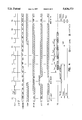
- FIG. 1 is a block diagram of a SDRAM according to the present invention.
- FIG. 2 is a timing diagram illustrating a four cycle read burst transfer operation.
- FIG. 3 is a timing diagram illustrating a four cycle write burst transfer operation.
- FIG. 4 is a timing diagram illustrating a four cycle read burst transfer operation implementing an AUTO-PRECHARGE command following a READ command.
- FIG. 5 is a simplified timing diagram illustrating the operation of a prior art SDRAM during interleaving between bank memory arrays during random accesses.
- FIG. 6 is a simplified timing diagram illustrating the SDRAM according to the present invention during interleaving between bank memory arrays during random accesses.
- SDRAM 20 A synchronous dynamic random access memory (SDRAM) according to the present invention is illustrated generally at 20 in FIG. 1 in block diagram form.
- Much of the circuitry of SDRAM 20 is similar to circuitry in known SDRAMs, such as the Micron Technology, Inc. MT48LC4M4R1 S 4 MEG X 4 SDRAM, which is described in detail in the corresponding Micron Technology, Inc. Functional Specification, which is incorporated herein by reference.
- SDRAM 20 includes a bank 0 memory array 22 and of bank 1 memory array 24 which both comprise storage cells organized in rows and columns for storing data.
- each bank memory array comprises four separate arrays of 2048 rows ⁇ 1024 columns.
- a typical SDRAM 20 provides optimum memory performance in a low voltage environment such as a 3.3 V environment.
- a system clock (CLK) signal is provided through a CLK input pin and a clock enable signal (CKE) is provided through a CKE input pin to SDRAM 20.
- CLK system clock
- CKE clock enable signal
- the CLK signal is activated and deactivated based on the state of the CKE signal. All the input and output signals of SDRAM 20, with the exception of the CKE input signal during power down and self refresh modes, are synchronized to the active going edge (the positive going edge in the embodiment illustrated in FIG. 1) of the CLK signal.
- a chip select (CS*) input pin inputs a CS* signal which enables, when low, and disables, when high a command decode 26.
- Command decode 26 is included in a command controller 28.
- Command decode 26 receives control signals including a row address strobe (RAS*) signal on a RAS* pin, column address strobe (CAS*) signal on a GAS* pin, and a write enable (WE*) signal on a WE* pin.
- RAS* row address strobe
- CAS* column address strobe
- WE* write enable
- Command decoder 26 decodes the RAS*, CAS*, and WE* signals to place command controller 28 in a particular command operation sequence.
- Command controller 28 controls the various circuitry of SDRAM 20 based on decoded commands such as during controlled reads or writes from or to bank 0 memory array 22 and bank 1 memory array 24.
- a bank address (BA) signal is provided on a BA input pin to define which bank memory array should be operated on by
- Address inputs bits are provided on input pins A0-A10. As described below, both the row and column address input bits are provided on the address input pins.
- data is supplied to SDRAM 20 via input/output pins (DQ1-DQ-4).
- data is clocked out of SDRAM 20 via input/output pins DQ1-DQ-4.
- An input/output mask signal is provided on a DQM input pin to provide non-persistent buffer control for a data-in-buffer 30 and a data-out buffer 32.
- SDRAM 20 must be powered-up and initialized in a predefined manner.
- both bank 0 and bank 1 memory arrays 22 and 24 must be precharged and placed in an idle state.
- the precharging of the bank memory arrays is preformed with a precharge command operation which is described in more detail below.
- two AUTO-REFRESH operations must be performed.
- Two refresh commands are typically available in SDRAM 20 which are an AUTO-REFRESH command and a SELF-REFRESH command.
- the AUTO-REFRESH and SELF-REFRESH commands are performed with refresh controller 34, self-refresh oscillator and timer 36, and refresh counter 38 in a manner known in the art to refresh the memory arrays.
- Mode register 40 is assumed to have an unknown state when SDRAM 20 is powered up. Consequently, before performing any operational command, mode register 40 must be set or programmed.
- Mode register 40 is typically a persistent register wherein once programmed, the mode register retains the program op-code until the mode register is reprograrraned or SDRAM 20 loses power. Most of the possible programmable options of SDRAM 20 are defined in the op-codes stored in mode register 40.
- mode register 40 is programmed by providing a desired op-code via the BA input pins and the A0-A10 address inputs, in conjunction with a SET MODE REGISTER command determined by CS*, RAS*, CAS*, and WE* being registered low.
- a valid ACTIVE command is initiated by command controller 28 with the CS* and RAS* signals low with the CAS* and WE* signals high on a rising edge of the CLK signal.
- the state of the BA signal determines which bank memory array to activate and address.
- a value representing a row address of the selected bank memory array is latched in a row address latch 42 in response to a clock signal generated from a clock generator circuit 44.
- the latched row address is provided to a row multiplexor 46 which provides a row address to row address buffers 48 to be provided to bank 0 memory array 22 or row address buffers 50 to be provided to bank 1 memory array 24 depending on the state of the BA signal.
- a row decoder 52 decodes the row address provided from row address buffers 48 to activate one of the 2,048 lines corresponding to the row address for read or write transfer operations, to thereby activate the corresponding row of storage cells in bank 0 memory array 22.
- Row decoder 54 similarly decodes the row address in row address buffer 50 to activate one of the 2,048 lines to bank 1 memory array 24 corresponding to the row address for read or write transfer operations, to thereby activate the corresponding row of storage cells in bank 1 memory array 24.
- a bank memory array In order to access a row once a row in the selected bank memory has been activated with the ACTIVE command, a bank memory array must be precharged with the below described PRECHARGE command or AUTO-PRECHARGE command before another ACTIVE command is applied to the bank memory array.
- a valid READ command is initiated with the CS* and CAS* signals low, and the RAS* and WE* signals high on a rising edge of the CLK signal.
- the READ command from command controller 28 controls a column address latch 56 which receives address bits A0-A9 and holds a value representing a column address of the bank memory array selected by the BA signal at the time the READ command is initiated.
- Column address latch 56 latches the column address in response to a clock signal generated by a clock generator 58.
- Address pin A10 provides an input path for a command signal which determines whether or not an AUTO-PRECHARGE command, described in detail below, is to be initiated automatically after the READ command.
- the READ command provided from command controller 28 also initiates a burst read cycle, described in detail below, by starting a burst counter 60.
- a column address buffer 62 receives the output of the burst counter 60 to provide the current count of the column address to a column decoder 64.
- Column decoder 64 activates four of the 1,024 ⁇ 4 lines, provided to sense amplifiers and input/output (I/O) gating circuit 66 and sense amplifiers and I/O gating circuit 68 corresponding to the current column address.
- Sense amplifiers and I/O gating circuits 66 and 68 operate in a manner known in the art to seine the data stored in the storage cells addressed by the active row decoder line and the active column decoder lines to provide the selected four bit byte of data from either bank 0 memory array 22 or bank 1 memory array 24 respectively to data-out buffer 32 during a read operation.
- Data-out buffer 32 provides the selected four bit byte of data to input/output data pins DQ1-DQ4.
- burst read having a length of four
- the initial column address stored in column address latch 56 is used to activate sense amplifiers and I/O gating circuits 66 or 68 during the first burst cycle of the burst read operation.
- burst counter 60 counts up from the column address stored in column address latch 56, as defined by a sequence type, to "burst" or clock-out the next three memory locations of dam.
- a full-page burst will wrap around and continually restart the "burst" operation until a BURST TERMINATION command or PRECHARGE command is indicated by command controller 28 or until interrupted with another burst operation.
- a valid WRITE command is initiated with the CS*, CAS*, and WE* signals low and the RAS* signal high on the rising edge of the CLK signal.
- the WRITE command provided from command controller 28 controls clock generator 58 to clock column address latch 55 which receives and holds a value representing a column address of the bank memory array selected by the state of the BA signal at the time the WRITE command is initiated, as indicated by the address provided on address input pins A0-A9.
- address pin A10 provides the additional feature to select whether or not the below described AUTO-PRECHARGE command is to be initiated following the WRITE command.
- Burst counter 50 initiates the burst write cycle.
- Column address buffer 62 receives the output of the burst counter 60 and provides the current column address to column decoder 64.
- Column decoder 64 activates four of the 1,024 ⁇ 4 lines to sense amplifiers and I/O gating circuits 66 and 68 corresponding to the column address to indicate where the incoming four bit byte of data is to be stored in either bank 0 memory array 22 or bank 1 memory array 24.
- data is provided on input/output pins DQ1-DQ4 to data-in buffer 30.
- Data in buffer 30 provides the input write data to a latch 70 corresponding to bank 0 memory array 22 and a latch 72 corresponding to bank 1 memory array 24.
- the four bit byte of input write data is provided from latch 70 or 72 to the selected bank memory array with seine amplifiers and I/O gating circuits 66 or 68 in a manner known in the art based on the activated four lines corresponding to the current column address.
- burst write operation of length four
- the first byte of data is stored at the memory array location addressed by the column address stored in column address latch 56.
- burst counter 60 counts up from the column address stored in column latch 56, as defined by the sequence type, to "burst" or clock in the data to be stored in the next three memory locations.
- a full page burst will wrap around and continue writing data until terminated by the BURST TERMINATION command, PRECHARGE command, or until interrupted with another burst operation.
- the burst read and write operation are controlled by the burst mode defined in mode register 40 which is programmable during the SET MODE REGISTER command.
- the burst operation provide for a continuous flow of data from or to the specified memory array location during read or write access. Burst lengths of 2, 4, 8, or full page (1,024) cycles are programmable into mode register 40 in one embodiment of SDRAM 20.
- a burst read/single write mode permits a write operation to be a burst length of one and yet allows the read operation to be the programmed burst length as defined in mode register 40.
- a burst sequence is a programmable feature programmed into mode register 40 during the SET MODE REGISTER command.
- two types of burst sequences are available for selection including a sequential sequence or an interleaving sequence.
- the sequential sequence bursts through sequential locations in one of the two bank memory arrays.
- the interleaving sequence interleaves between bank 0 memory array 22 and bank 1 memory array 24.
- both the sequential and interleaving sequences support bursts of 2, 4, and 8 cycles.
- the sequential sequence supports full page length burst cycles.
- the PRECHARGE command operation deactivates and precharges the bank memory array selected by the state of the BA signal at the time the PRECHARGE command is initiated. In this way, the row previously accessed is deactivated and precharged so that row may be refreshed or another row accessed. Once a bank memory array has been precharged, that bank memory array is in an idle state and must be activated prior to another READ command or WRITE command being issued to that bank memory array. In the preferred embodiment of the SDRAM 20, multiple READ and WRITE commands do not require precharging between each command provided the same row is being accessed.
- the PRECHARGE command allows either one or both banks to be precharged. Individual bank precharging is performed if the value on address input pin A10 is registered low at the time the PRECHARGE command is initiated. During individual bank precharging, the state of the BA signal defines which bank is precharged. Both banks are precharged when A10 is registered high at the time the PRECHARGE command is initiated. If A10 is registered high at the time the PRECHARGE command is initiated, BA is treated as a "don't care.”
- the bank memory array to be accessed is determined by the registering of the BA signal at the initiation of the command.
- Bank 0 memory array 22 is selected if the value of the BA signal is registered low and bank 1 memory array 24 is selected if the value of the BA signal is registered high.
- the BA signal determines the selection of one of the banks during a PRECHARGE command only when the value on input pin A10 is low. If the value on input pin A10 is high during the PRECHARGE command, BA becomes a "don't care.”
- Precharging a bank memory array can, in most cases, be hidden due to the dual bank structure of SDRAM 20.
- a PRECHARGE command is issued to the bank memory array not being accessed while the bank memory array being accessed is in a burst mode.
- the PRECHARGE command may be initiated up to one clock cycle prior to the last data-out during a read operation, provided that the read latency is two or more clocks. When the read latency is one clock, the PRECHARGE command may only be issued when the final data-out is available. In any case, at least one clock cycle of the precharge time T RP must occur during the cycle the last data-out is being held valid. That is, one of two or two of three clock cycles of the precharge time may be hidden provided the read latency is two or more. Otherwise, only one precharge clock may be hidden.
- WRITE commands require a write recovery time (T WR ) from the last data-in element to the beginning of the PRECHARGE command when the same bank memory array is going from a write command to a PRECHARGE command.
- An AUTO-PRECHARGE command is a non-persistent feature in SDRAM 20 which performs all of the same individual bank precharge functions described above for the PRECHARGE command.
- the AUTO-PRECHARGE command feature of the preferred embodiment of SDRAM 20 permits a use to program a READ command or WRITE command that automatically performs a precharge upon the completion of the READ command or the WRITE command.
- a manual PRECHARGE command does not need to be issued during the functional operation of SDRAM 20.
- the AUTO-PRECHARGE command insures that the precharge is initiated at the earliest, valid stage within a burst cycle. The user is not allowed to issue another command until the precharged time (t RP ) is completed. Therefore, when an AUTO-PRECHARGE command is employed in SDRAM 20, the selected bank memory array must not be accessed again until t RP , is complete. For example, if a read of two cycles is selected and three clock periods are required to satisfy t RP the bank memory array cannot be accessed during the two clocks following the completion of a burst operation.
- the bank memory array cannot be accessed during the one clock cycle following the completion of the burst, provided that the read latency is two or more clocks, otherwise, the bank memory array cannot be accessed during the two clocks following the completion of the burst cycle.
- the read latency is a programmable feature of SDRAM 20 defined in mode register 40 during the SET MODE REGISTER command. Typically, read latencies of 1,2, or 3 clocks are available. The read latency guarantees at which clock the data will become available regardless of the system clock rate. Data can be made available on the input/output pins DQ1-DQ4 up to one clock cycle less than the read latency, depending on the frequency of the system clock. A read latency of two clocks programmed with a cycle rate which is greater than the minimum access time will provide data almost immediately after the first clock.
- a no operation (NOP) command can be provided to SDRAM 20 to prevent other unwanted commands from being registered during idle or wait states.
- a four cycle burst read operation is illustrated in timing diagram form in FIG. 2.
- the system clock cycle time is indicated by t CK .
- the time from the initiation of an ACTIVE command to the initiation of a READ command is representing by t RCD and represents two clock cycles, such a between time t 0 and time t 2 .
- the total read burst transfer cycle period is represented by t RC and represents nine clock cycles as illustrated in FIG. 2.
- the total ACTIVE command period, wherein the row address strobe is active, is represented by t RAS , and represents four clock cycles as illustrated in FIG. 2.
- the READ access time for each cycle burst in represented by t AC .
- the time from the initiation of the READ command to the DQ clock first data-out cycle is represented by t AA and indicates the column address strobe latency period and is two clock periods as illustrated in FIG. 2.
- the PRECHARGE command period (t RP ) is three system clock cycles as illustrated in FIG. 2.
- an ACTIVE command is initiated by command controller 28 at time t 0 ; the corresponding READ command is initiated at time t 2 ; the first cycle burst of data is output at time t 4 ; and the last of the four cycle data bursts is output at time t 7 .
- a PRECHARGE command is initiated when the second to last data burst is output, and the next ACTIVE command is initiated at time t 9 , three clock cycles after the PRECHARGE command at time t 6 .
- FIG. 3 A four cycle burst write transfer operation is illustrated in timing diagram form in FIG. 3.
- the timing diagram of FIG. 3 is similar to the timing diagram of FIG. 2 illustrating the four cycle READ burst transfer operation. Therefore, only the differences between the WRITE and READ commands are now described.
- the data-in setup time is represented by t DS
- the data-in hold time is represented by t DH .
- the write recovery time is indicated by t WR , which represents one clock cycle in FIG. 3 between t 5 and t 6 .
- the time from when the WRITE command is initiated at t 2 to when the write recovery time is completed after four data bursts have been written into one of the bank memory arrays represents four clock cycles as illustrated in FIG. 3 between t 2 and t 6 .
- the total command period (t RC ) is again equal to nine clock cycles for the four cycle write burst transfer operation.
- FIGS. 2 and 3 represent a four cycle burst transfer operation, but as described above SDRAM 20 preferably can be programmed to perform 2, 4, 8, or full page cycle burst operations and the present invention is not limited to a four burst transfer operation.
- FIG. 4 A four cycle read burst transfer operation which utilizes a programmed READ command which automatically issues an AUTO-PRECHARGE command without having to issue and an actual PRECHARGE command is illustrated in FIG. 4 in timing diagram form.
- FIG. 4 is similar to FIG. 2 except at time t 6 a NOP command is issued rather than the PRECHARGE command since at time t 6 the AUTO.0-PRECHARGE command is internally performed.
- FIG. 3 illustrates an AUTO-PRECHARGE command following a WRITE command.
- SDRAM's such as SDRAM 20, which comprise two bank memory arrays
- interleaving between the two open bank memory arrays increases the probability of "Page Hits.”
- the interleaving between open bank memory arrays coupled with the high-speed burst mode READ command and WRITE command operations may, in many cases, provide a "seamless" flow of data.
- Prior art SDRAMs require an extra dead cycle or wait cycle when interleaving between bank memory arrays when performing read or write burst transfer operations comprising random accesses wherein new pages are accessed.
- SDRAM 20 includes a special program option programmed into mode register 40 during the SET MODE REGISTER command to solve this problem to thereby reduce and improve the cycle time on random interleave accesses to eliminate the extra dead cycle during read or write burst transfer operations.
- the special program option in mode register 40 causes command controller 28 to internally generate an AUTO-PRECHARGE command to the bank memory array which is currently bursting, even on full page read or write burst transfer operations, in the same system clock cycle that the other bank memory array receives either a READ or WRITE command.
- FIG. 5 represents a simplified timing diagram to illustrate the above described problem in a conventional SDRAM interleaving sequence for a READ command burst transfer operation comprising random accesses.
- This interleaving sequence is shown for a four cycle read burst transfer operation for illustrative purposes only, and could be shown for any length burst including full page.
- the illustrated example could also be applied to any WRITE command burst transfer operation.
- the ACTIVE command is initiated.
- the READ command is initiated for bank 0 memory array 22.
- data from the first of the four burst cycles is output from the conventional SDRAM.
- the data from the other three burst cycles is read from bank 0 memory array 22.
- an ACTIVE command is initiated in bank 1 memory array 24.
- a PRECHARGE command is initiated in bank 0 memory array 22.
- a READ command is initiated in bank 1 memory array 24.
- This pattern of interleaving repeats with data being output from conventional SDRAM at time T 10 , T 11 , T 12 , and T 13 from bank 1 memory array 24 resulting from the READ command at time t 8 .
- An ACTIVE command is initiated at time t 11 in bank 0 memory array 22.
- the PRECHARGE command is initiated at time t 12 for bank 1 memory array 24.
- the READ command is again initiated at time t 13 for bank 0 memory array 22 after the PRECHARGE command in bank 1 memory array 24.
- data is output at time t 15 , t 16 ,t 17 , and t 18 .
- an ACTIVE command is initiated for bank 1 memory array 24 at time t 15 and the corresponding READ command is initiated at time t 18 for bank 1 memory array 24.
- FIG. 6 illustrates the operation of SDRAM 20 according to the present invention with the additional special program option in mode register 40 to eliminate the wasted cycle between the PRECHARGE command at time t 7 and the READ command at time t 8 .
- the ACTIVE command is again initiated at time t 1 for bank 0 memory array 22, and the READ command is initiated at time t 3 for bank memory array 22.
- an ACTIVE command is then initiated for bank 1 memory array 24 at time t 5 .
- the ACTIVE command initiated at time t 5 for bank 1 memory array 24 also automatically triggers command controller 28 to internally initiate an AUTO-PRECHARGE command at time t 7 .
- the READ command initiated for bank 1 memory array 24 at time t 7 does not conflict with the AUTO-PRECHARGE command initiated as a result of the ACTIVE command at time t 5 because the command decoder does not need to decode the CS*, WE*, CAS*, WAS*, and BA signals for the internally and automatically initiated AUTO-PRECHARGE command. In this way, the switching between bank 0 memory array 22 and bank 1 memory array 24 is achieved in one less clock cycle.
- the next ACTIVE command for the bank 0 memory array 22 is initiated at time t 10 . Since a READ command must follow two cycles later than the ACTIVE command, there is no conflict between the ACTIVE command at time t 10 , the PRECHARGE command at time t 11 , and the READ command at time t 12 , as far as inputting the CS*, WE*, CAS*, WAS*, and BA signals to be decoded by command decoder 26.
- command controller 28 analyzes the BA signal and the command input signals WE*, CAS*, and RAS* along with CS* signal to initiate the AUTO-PRECHARGE command if the new ACTIVE command operation is to be performed in a different bank memory array than the previous READ or WRITE command transfer operation.
- a special ACTIVE command is programmed into mode register 40 during the SET MODE REGISTER command at start-up. This special ACTIVE command needs to be applied by the user just as with the special programmable READ or WRITE command to initiate an AUTO-PRECHARGE command. In this preferred embodiment, the ACTIVE command at time t 5 is replaced by the special ACTIVE command.
- the user is not required to initiate a special ACTIVE command manually when switching bank memory arrays, but does need to program, at start up, the initiation of the AUTO-PRECHARGE command based on an ACTIVE command when switching between bank memory arrays.
- the special. ACTIVE command of the second preferred embodiment of the present invention the user of SDRAM 20 needs to manually provide the special ACTIVE command in place of the normal ACTIVE command when switching banks to take advantage of the AUTO-PRECHARGE command to the other bank memory array based on the special ACTIVE command.
- the AUTO-PRECHARGE command and the transfer READ or WRITE transfer operation can be initiated by command controller 28 in the same the system clock cycle.
- the above described AUTO-PRECHARE command initiated at time t 7 to the bank 0 memory array during the READ or WRITE transfer command to the bank 1 memory array, as illustrated in FIG. 6, is not initiated based on the ACTIVE command at time t 5 . Instead the AUTO-PRECHARGE command is initiated at time t 7 based on a special READ or WRITE transfer command initiated at time t 7 .
- the special READ or WRITE command needs to be decoded by command decoder 26 at time t 7 , because both the transfer operation and the precharge operation are initiated at time t 7 as a result of the CS*, WE*, CAS*, and RAS* command signals indicating a special READ or WRITE command.
- the special READ and WRITE commands are programmed into mode register 40 during the SET MODE REGISTER command at start-up.
- the special READ or WRITE command needs to be manually applied by the user in place of the normal READ or WRITE command to initiate an AUTO-PRECHARGE to the other bank memory array command in this alterative form of the present invention.
- the present invention is not limited to a SDRAM having only two bank memory arrays.
- SDRAM 20 according to the present invention is alternatively embodied in a SDRAM having more than the shown bank 0 and bank 1 memory arrays, such as four (banks 0-3) or eight (banks 0-7) bank memory arrays.
- the above described AUTO-PRECHARGE command operation to the bank 0 memory array during the READ or WRITE transfer command to the bank 1 memory array, as illustrated in FIG. 6, is applied to any selected two of the multiple bank memory arrays.
- an AUTO-PRECHARGE is initiated at time t 7 , represented in FIG. 6 in a predefined closest bank memory array to the bank memory array having the READ or WRITE command initiated at time t 7 .
- the AUTO-PRECHARGE command applied at time t 7 is initiated in the bank 1 memory array, or if the bank 4 memory array has a READ or WRITE transfer command operation initiated at time t 7 , the AUTO-PRECHARGE command applied at time t 7 is initiated in the bank 3 memory array.
- an AUTO-PRECHARGE is initiated at time t 7 , represented in FIG. 6, in the most recently accessed bank memory array instead of the predefined closest bank memory array.
- the AUTO-PRECHARGE command applied at time t 7 is initiated in the bank 2 memory array (i.e., the previously accessed bank memory array) instead of the bank 3 memory array (i.e., the predefined closest bank memory array).
- the wasted clock cycle, illustrated at t 9 in FIG. 5 for a conventional SDRAM is eliminated to improve cycle time on random interleave accesses.
- the interleave transfer operation sequence to read data from or write data to both of the bank memory arrays is performed in 12 system clock cycles in SDRAM 20 of the present invention, instead of the 13 clock cycles required to perform the same interleave transfer operation sequence in the prior art SDRAM illustrated in FIG. 5. In other words, this results in a 8% performance increase on either READ or WRITE transfer operations during an random interleave access.
Abstract
Description
Claims (42)
Priority Applications (1)
| Application Number | Priority Date | Filing Date | Title |
|---|---|---|---|
| US08/480,154 US5636173A (en) | 1995-06-07 | 1995-06-07 | Auto-precharge during bank selection |
Applications Claiming Priority (1)
| Application Number | Priority Date | Filing Date | Title |
|---|---|---|---|
| US08/480,154 US5636173A (en) | 1995-06-07 | 1995-06-07 | Auto-precharge during bank selection |
Publications (1)
| Publication Number | Publication Date |
|---|---|
| US5636173A true US5636173A (en) | 1997-06-03 |
Family
ID=23906868
Family Applications (1)
| Application Number | Title | Priority Date | Filing Date |
|---|---|---|---|
| US08/480,154 Expired - Lifetime US5636173A (en) | 1995-06-07 | 1995-06-07 | Auto-precharge during bank selection |
Country Status (1)
| Country | Link |
|---|---|
| US (1) | US5636173A (en) |
Cited By (95)
| Publication number | Priority date | Publication date | Assignee | Title |
|---|---|---|---|---|
| US5748560A (en) * | 1995-12-25 | 1998-05-05 | Mitsubishi Denki Kabushiki Kaisha | Synchronous semiconductor memory device with auto precharge operation easily controlled |
| US5757715A (en) * | 1994-04-15 | 1998-05-26 | Micron Technology, Inc. | Method for initializing and reprogramming a control operation feature of a memory device |
| US5790468A (en) * | 1996-06-03 | 1998-08-04 | Hyundai Electronics Industries Co., Ltd. | Refresh counter for synchronous dynamic random access memory and method of testing the same |
| US5818777A (en) * | 1997-03-07 | 1998-10-06 | Micron Technology, Inc. | Circuit for implementing and method for initiating a self-refresh mode |
| US5838177A (en) * | 1997-01-06 | 1998-11-17 | Micron Technology, Inc. | Adjustable output driver circuit having parallel pull-up and pull-down elements |
| US5870347A (en) * | 1997-03-11 | 1999-02-09 | Micron Technology, Inc. | Multi-bank memory input/output line selection |
| US5872736A (en) * | 1996-10-28 | 1999-02-16 | Micron Technology, Inc. | High speed input buffer |
| GB2332539A (en) * | 1997-12-17 | 1999-06-23 | Fujitsu Ltd | Accessing random access memories |
| US5920518A (en) * | 1997-02-11 | 1999-07-06 | Micron Technology, Inc. | Synchronous clock generator including delay-locked loop |
| US5923594A (en) * | 1998-02-17 | 1999-07-13 | Micron Technology, Inc. | Method and apparatus for coupling data from a memory device using a single ended read data path |
| US5926047A (en) * | 1997-08-29 | 1999-07-20 | Micron Technology, Inc. | Synchronous clock generator including a delay-locked loop signal loss detector |
| US5940608A (en) * | 1997-02-11 | 1999-08-17 | Micron Technology, Inc. | Method and apparatus for generating an internal clock signal that is synchronized to an external clock signal |
| US5946244A (en) * | 1997-03-05 | 1999-08-31 | Micron Technology, Inc. | Delay-locked loop with binary-coupled capacitor |
| US5949254A (en) * | 1996-11-26 | 1999-09-07 | Micron Technology, Inc. | Adjustable output driver circuit |
| US5953284A (en) * | 1997-07-09 | 1999-09-14 | Micron Technology, Inc. | Method and apparatus for adaptively adjusting the timing of a clock signal used to latch digital signals, and memory device using same |
| US5956502A (en) * | 1997-03-05 | 1999-09-21 | Micron Technology, Inc. | Method and circuit for producing high-speed counts |
| US5959929A (en) * | 1997-12-29 | 1999-09-28 | Micron Technology, Inc. | Method for writing to multiple banks of a memory device |
| US5963481A (en) * | 1998-06-30 | 1999-10-05 | Enhanced Memory Systems, Inc. | Embedded enhanced DRAM, and associated method |
| US5973993A (en) * | 1998-02-27 | 1999-10-26 | Micron Technology, Inc. | Semiconductor memory burst length count determination detector |
| US5982697A (en) * | 1996-12-02 | 1999-11-09 | Micron Technology, Inc. | Method for initializing and reprogramming a control operation feature of a memory device |
| US6009501A (en) * | 1997-06-18 | 1999-12-28 | Micron Technology, Inc. | Method and apparatus for local control signal generation in a memory device |
| US6011732A (en) | 1997-08-20 | 2000-01-04 | Micron Technology, Inc. | Synchronous clock generator including a compound delay-locked loop |
| US6014759A (en) * | 1997-06-13 | 2000-01-11 | Micron Technology, Inc. | Method and apparatus for transferring test data from a memory array |
| US6016282A (en) | 1998-05-28 | 2000-01-18 | Micron Technology, Inc. | Clock vernier adjustment |
| USRE36532E (en) * | 1995-03-02 | 2000-01-25 | Samsung Electronics Co., Ltd. | Synchronous semiconductor memory device having an auto-precharge function |
| US6029250A (en) | 1998-09-09 | 2000-02-22 | Micron Technology, Inc. | Method and apparatus for adaptively adjusting the timing offset between a clock signal and digital signals transmitted coincident with that clock signal, and memory device and system using same |
| US6032220A (en) * | 1997-07-18 | 2000-02-29 | Micron Technology, Inc. | Memory device with dual timing and signal latching control |
| US6044429A (en) * | 1997-07-10 | 2000-03-28 | Micron Technology, Inc. | Method and apparatus for collision-free data transfers in a memory device with selectable data or address paths |
| US6052134A (en) * | 1997-12-22 | 2000-04-18 | Compaq Computer Corp. | Memory controller and method for dynamic page management |
| US6064619A (en) * | 1997-06-30 | 2000-05-16 | Hyundai Electronics Industries Co., Ltd. | Synchronous dynamic random access memory in a semiconductor memory device |
| US6101152A (en) * | 1990-04-18 | 2000-08-08 | Rambus Inc. | Method of operating a synchronous memory device |
| US6101197A (en) * | 1997-09-18 | 2000-08-08 | Micron Technology, Inc. | Method and apparatus for adjusting the timing of signals over fine and coarse ranges |
| US6115318A (en) | 1996-12-03 | 2000-09-05 | Micron Technology, Inc. | Clock vernier adjustment |
| US6141290A (en) * | 1997-08-22 | 2000-10-31 | Micron Technology, Inc. | Method and apparatus for controlling the operation of an integrated circuit responsive to out-of-synchronism control signals |
| US6173432B1 (en) | 1997-06-20 | 2001-01-09 | Micron Technology, Inc. | Method and apparatus for generating a sequence of clock signals |
| US6185150B1 (en) | 1998-11-27 | 2001-02-06 | Kabushiki Kaisha Toshiba | Clock-synchronous system |
| US6215711B1 (en) * | 1998-12-31 | 2001-04-10 | Hyundai Electronics Industries Co., Ltd. | Row address strobe signal generating device |
| US6223301B1 (en) * | 1997-09-30 | 2001-04-24 | Compaq Computer Corporation | Fault tolerant memory |
| US6247088B1 (en) | 1998-05-08 | 2001-06-12 | Lexmark International, Inc. | Bridgeless embedded PCI computer system using syncronous dynamic ram architecture |
| US6269451B1 (en) | 1998-02-27 | 2001-07-31 | Micron Technology, Inc. | Method and apparatus for adjusting data timing by delaying clock signal |
| US6279090B1 (en) | 1998-09-03 | 2001-08-21 | Micron Technology, Inc. | Method and apparatus for resynchronizing a plurality of clock signals used in latching respective digital signals applied to a packetized memory device |
| US6298413B1 (en) | 1998-11-19 | 2001-10-02 | Micron Technology, Inc. | Apparatus for controlling refresh of a multibank memory device |
| US6301183B1 (en) * | 2000-02-29 | 2001-10-09 | Enhanced Memory Systems, Inc. | Enhanced bus turnaround integrated circuit dynamic random access memory device |
| US6314527B1 (en) * | 1998-03-05 | 2001-11-06 | Micron Technology, Inc. | Recovery of useful areas of partially defective synchronous memory components |
| US6326810B1 (en) | 1996-11-04 | 2001-12-04 | Micron Technology, Inc. | Adjustable output driver circuit |
| US6330636B1 (en) | 1999-01-29 | 2001-12-11 | Enhanced Memory Systems, Inc. | Double data rate synchronous dynamic random access memory device incorporating a static RAM cache per memory bank |
| US6332183B1 (en) * | 1998-03-05 | 2001-12-18 | Micron Technology, Inc. | Method for recovery of useful areas of partially defective synchronous memory components |
| US6333888B1 (en) * | 1999-04-23 | 2001-12-25 | Nec Corporation | Semiconductor memory device |
| US6338127B1 (en) | 1998-08-28 | 2002-01-08 | Micron Technology, Inc. | Method and apparatus for resynchronizing a plurality of clock signals used to latch respective digital signals, and memory device using same |
| US6347357B1 (en) | 1992-01-22 | 2002-02-12 | Enhanced Memory Systems, Inc. | Enhanced DRAM with embedded registers |
| US6349399B1 (en) | 1998-09-03 | 2002-02-19 | Micron Technology, Inc. | Method and apparatus for generating expect data from a captured bit pattern, and memory device using same |
| US6374360B1 (en) | 1998-12-11 | 2002-04-16 | Micron Technology, Inc. | Method and apparatus for bit-to-bit timing correction of a high speed memory bus |
| US6381708B1 (en) | 1998-04-28 | 2002-04-30 | Micron Technology, Inc. | Method for decoding addresses for a defective memory array |
| US6381707B1 (en) | 1998-04-28 | 2002-04-30 | Micron Technology, Inc. | System for decoding addresses for a defective memory array |
| US6392948B1 (en) * | 1996-08-29 | 2002-05-21 | Micron Technology, Inc. | Semiconductor device with self refresh test mode |
| US6405280B1 (en) | 1998-06-05 | 2002-06-11 | Micron Technology, Inc. | Packet-oriented synchronous DRAM interface supporting a plurality of orderings for data block transfers within a burst sequence |
| US20020083383A1 (en) * | 2000-12-27 | 2002-06-27 | Winbond Electronics Corp. | Method for testing memories with seamless data input/output by interleaving seamless bank commands |
| US6426909B1 (en) * | 2000-11-17 | 2002-07-30 | Fujitsu Limited | Semiconductor memory |
| GB2371662A (en) * | 2000-10-24 | 2002-07-31 | Hynix Semiconductor Inc | Semiconductor memory with precharging interrupt signal and predecoding |
| US6430696B1 (en) | 1998-11-30 | 2002-08-06 | Micron Technology, Inc. | Method and apparatus for high speed data capture utilizing bit-to-bit timing correction, and memory device using same |
| US6438055B1 (en) * | 1999-10-20 | 2002-08-20 | Fujitsu Limited | Dynamic memory circuit with automatic refresh function |
| US6496876B1 (en) | 1998-12-21 | 2002-12-17 | Micron Technology, Inc. | System and method for storing a tag to identify a functional storage location in a memory device |
| US6507526B2 (en) * | 2000-06-28 | 2003-01-14 | Kabushiki Kaisha Toshiba | Semiconductor memory with improved auto precharge |
| US6526471B1 (en) * | 1998-09-18 | 2003-02-25 | Digeo, Inc. | Method and apparatus for a high-speed memory subsystem |
| EP1291878A2 (en) | 2001-09-07 | 2003-03-12 | Philips Corporate Intellectual Property GmbH | Control device for control of burst access |
| US6567338B1 (en) | 1996-04-19 | 2003-05-20 | Integrated Device Technology, Inc. | Fully synchronous pipelined RAM |
| US6578157B1 (en) | 2000-03-06 | 2003-06-10 | Micron Technology, Inc. | Method and apparatus for recovery of useful areas of partially defective direct rambus rimm components |
| US6587918B1 (en) * | 1998-11-19 | 2003-07-01 | Micron Technology, Inc. | Method for controlling refresh of a multibank memory device |
| US6591354B1 (en) | 1998-02-23 | 2003-07-08 | Integrated Device Technology, Inc. | Separate byte control on fully synchronous pipelined SRAM |
| US20030167374A1 (en) * | 1999-07-02 | 2003-09-04 | Stanley A. Hronik | Double data rate synchronous sram with 100% bus utilization |
| US6643212B1 (en) * | 2002-04-18 | 2003-11-04 | United Memories, Inc. | Simultaneous function dynamic random access memory device technique |
| US20030225987A1 (en) * | 2002-05-28 | 2003-12-04 | Micron Technology, Inc. | Software command sequence for optimized power consumption |
| DE10234679A1 (en) * | 2002-07-30 | 2004-02-19 | Infineon Technologies Ag | Memory device such as a dram and operating process has unit which only drives busses when an activation signal is active |
| US20040039883A1 (en) * | 2002-08-26 | 2004-02-26 | Laberge Paul A | Modified persistent auto precharge command protocol system and method for memory devices |
| US20040120210A1 (en) * | 2002-12-20 | 2004-06-24 | Lee Dong-Yang | Semiconductor memory devices with delayed auto-precharge function and associated methods of auto-precharging semiconductor memory devices |
| US6771553B2 (en) | 2001-10-18 | 2004-08-03 | Micron Technology, Inc. | Low power auto-refresh circuit and method for dynamic random access memories |
| US20040184324A1 (en) * | 2002-06-07 | 2004-09-23 | Pax George E | Reduced power registered memory module and method |
| US6801989B2 (en) | 2001-06-28 | 2004-10-05 | Micron Technology, Inc. | Method and system for adjusting the timing offset between a clock signal and respective digital signals transmitted along with that clock signal, and memory device and computer system using same |
| US20050071541A1 (en) * | 2003-09-30 | 2005-03-31 | Osborne Randy B. | Method and apparatus for implicit DRAM precharge |
| GB2407422A (en) * | 2000-10-31 | 2005-04-27 | Hynix Semiconductor Inc | Semiconductor memory device |
| US20050166007A1 (en) * | 2004-01-27 | 2005-07-28 | Seiko Epson Corporation | Information processing apparatus and method of accessing memory |
| US20050268024A1 (en) * | 2004-05-28 | 2005-12-01 | Samsung Electronics Co., Ltd. | Memory controller for use in multi-thread pipeline bus system and memory control method |
| US20060189690A1 (en) * | 2003-11-14 | 2006-08-24 | Dunham Charles F | Compounds to affect insect behavior and/or bird behavior |
| US20070121399A1 (en) * | 2005-11-30 | 2007-05-31 | Bains Kuljit S | Semiconductor memory devices and systems, and methods of using having reduced timers and registers |
| US7269765B1 (en) | 2000-04-13 | 2007-09-11 | Micron Technology, Inc. | Method and apparatus for storing failing part locations in a module |
| US20070242547A1 (en) * | 2006-04-14 | 2007-10-18 | Hynix Semiconductor Inc. | Self refresh operation of semiconductor memory device |
| US20090129178A1 (en) * | 1997-10-10 | 2009-05-21 | Barth Richard M | Integrated Circuit Memory Device Having Delayed Write Timing Based on Read Response Time |
| US20090303824A1 (en) * | 2005-10-31 | 2009-12-10 | Mosaid Technologies Incorporated | Dynamic random access memory device and method for self-refreshing memory cells |
| US20100202226A1 (en) * | 2009-02-12 | 2010-08-12 | Hynix Semiconductor Inc. | Bank precharge signal generation circuit |
| US20100214864A1 (en) * | 2007-09-06 | 2010-08-26 | Micron Technology, Inc. | Memory device command decoding system and memory device and processor-based system using same |
| US8107580B2 (en) | 1999-03-01 | 2012-01-31 | Round Rock Research, Llc | Method and apparatus for generating a phase dependent control signal |
| US8181092B2 (en) | 2003-06-12 | 2012-05-15 | Round Rock Research, Llc | Dynamic synchronization of data capture on an optical or other high speed communications link |
| US20140362656A1 (en) * | 2013-06-06 | 2014-12-11 | Etron Technology, Inc. | Memory with low current consumption and method for reducing current consumption of a memory |
| US20150049570A1 (en) * | 2013-08-16 | 2015-02-19 | Sung-Hyun Lee | Memory device, memory system including the same, operating method thereof |
| US10635357B2 (en) | 2018-07-03 | 2020-04-28 | Nvidia Corporation | Method for overlapping memory accesses |
Citations (8)
| Publication number | Priority date | Publication date | Assignee | Title |
|---|---|---|---|---|
| US4667313A (en) * | 1985-01-22 | 1987-05-19 | Texas Instruments Incorporated | Serially accessed semiconductor memory with tapped shift register |
| US5208779A (en) * | 1991-04-15 | 1993-05-04 | Micron Technology, Inc. | Circuit for providing synchronous refresh cycles in self-refreshing interruptable DRAMs |
| US5229969A (en) * | 1991-04-15 | 1993-07-20 | Micron Technology, Inc. | Method for synchronizing refresh cycles in self-refreshing DRAMs having timing circuit shutdown |
| US5229970A (en) * | 1991-04-15 | 1993-07-20 | Micron Technology, Inc. | Circuit for synchronizing refresh cycles in self-refreshing drams having timing circuit shutdown |
| US5257233A (en) * | 1990-10-31 | 1993-10-26 | Micron Technology, Inc. | Low power memory module using restricted RAM activation |
| US5335201A (en) * | 1991-04-15 | 1994-08-02 | Micron Technology, Inc. | Method for providing synchronous refresh cycles in self-refreshing interruptable DRAMs |
| US5412613A (en) * | 1993-12-06 | 1995-05-02 | International Business Machines Corporation | Memory device having asymmetrical CAS to data input/output mapping and applications thereof |
| US5493535A (en) * | 1993-12-24 | 1996-02-20 | Samsung Electronics Co., Ltd. | Memory addressing method and apparatus therefor |
-
1995
- 1995-06-07 US US08/480,154 patent/US5636173A/en not_active Expired - Lifetime
Patent Citations (8)
| Publication number | Priority date | Publication date | Assignee | Title |
|---|---|---|---|---|
| US4667313A (en) * | 1985-01-22 | 1987-05-19 | Texas Instruments Incorporated | Serially accessed semiconductor memory with tapped shift register |
| US5257233A (en) * | 1990-10-31 | 1993-10-26 | Micron Technology, Inc. | Low power memory module using restricted RAM activation |
| US5208779A (en) * | 1991-04-15 | 1993-05-04 | Micron Technology, Inc. | Circuit for providing synchronous refresh cycles in self-refreshing interruptable DRAMs |
| US5229969A (en) * | 1991-04-15 | 1993-07-20 | Micron Technology, Inc. | Method for synchronizing refresh cycles in self-refreshing DRAMs having timing circuit shutdown |
| US5229970A (en) * | 1991-04-15 | 1993-07-20 | Micron Technology, Inc. | Circuit for synchronizing refresh cycles in self-refreshing drams having timing circuit shutdown |
| US5335201A (en) * | 1991-04-15 | 1994-08-02 | Micron Technology, Inc. | Method for providing synchronous refresh cycles in self-refreshing interruptable DRAMs |
| US5412613A (en) * | 1993-12-06 | 1995-05-02 | International Business Machines Corporation | Memory device having asymmetrical CAS to data input/output mapping and applications thereof |
| US5493535A (en) * | 1993-12-24 | 1996-02-20 | Samsung Electronics Co., Ltd. | Memory addressing method and apparatus therefor |
Cited By (204)
| Publication number | Priority date | Publication date | Assignee | Title |
|---|---|---|---|---|
| US6101152A (en) * | 1990-04-18 | 2000-08-08 | Rambus Inc. | Method of operating a synchronous memory device |
| US6347357B1 (en) | 1992-01-22 | 2002-02-12 | Enhanced Memory Systems, Inc. | Enhanced DRAM with embedded registers |
| US7370140B2 (en) | 1992-01-22 | 2008-05-06 | Purple Mountain Server Llc | Enhanced DRAM with embedded registers |
| US20090122619A1 (en) * | 1992-01-22 | 2009-05-14 | Purple Mountain Server Llc | Enhanced DRAM with Embedded Registers |
| US5757715A (en) * | 1994-04-15 | 1998-05-26 | Micron Technology, Inc. | Method for initializing and reprogramming a control operation feature of a memory device |
| USRE36532E (en) * | 1995-03-02 | 2000-01-25 | Samsung Electronics Co., Ltd. | Synchronous semiconductor memory device having an auto-precharge function |
| US5748560A (en) * | 1995-12-25 | 1998-05-05 | Mitsubishi Denki Kabushiki Kaisha | Synchronous semiconductor memory device with auto precharge operation easily controlled |
| US6785188B2 (en) | 1996-04-19 | 2004-08-31 | Integrated Device Technology, Inc. | Fully synchronous pipelined RAM |
| US6567338B1 (en) | 1996-04-19 | 2003-05-20 | Integrated Device Technology, Inc. | Fully synchronous pipelined RAM |
| US5790468A (en) * | 1996-06-03 | 1998-08-04 | Hyundai Electronics Industries Co., Ltd. | Refresh counter for synchronous dynamic random access memory and method of testing the same |
| US6545925B2 (en) | 1996-08-29 | 2003-04-08 | Micron Technology, Inc. | Semiconductor device with self refresh test mode |
| US6816426B2 (en) | 1996-08-29 | 2004-11-09 | Micron Technology, Inc. | Semiconductor device with self refresh test mode |
| US6856567B2 (en) | 1996-08-29 | 2005-02-15 | Micron Technology, Inc. | Semiconductor device with self refresh test mode |
| US6392948B1 (en) * | 1996-08-29 | 2002-05-21 | Micron Technology, Inc. | Semiconductor device with self refresh test mode |
| US6928019B2 (en) | 1996-08-29 | 2005-08-09 | Micron Technology, Inc. | Semiconductor device with self refresh test mode |
| US20050249012A1 (en) * | 1996-08-29 | 2005-11-10 | Lee Terry R | Semiconductor device with self refresh test mode |
| US20080279022A1 (en) * | 1996-08-29 | 2008-11-13 | Micron Technology, Inc. | Semiconductor device with self refresh test mode |
| US7428181B2 (en) | 1996-08-29 | 2008-09-23 | Micron Technology, Inc. | Semiconductor device with self refresh test mode |
| US20040213061A1 (en) * | 1996-08-29 | 2004-10-28 | Lee Terry R. | Semiconductor device with self refresh test mode |
| US8687446B2 (en) | 1996-08-29 | 2014-04-01 | Round Rock Research, Llc | Semiconductor device with self refresh test mode |
| US20050265105A1 (en) * | 1996-08-29 | 2005-12-01 | Lee Terry R | Semiconductor device with self refresh test mode |
| US5872736A (en) * | 1996-10-28 | 1999-02-16 | Micron Technology, Inc. | High speed input buffer |
| US6437600B1 (en) | 1996-11-04 | 2002-08-20 | Micron Technology, Inc. | Adjustable output driver circuit |
| US6326810B1 (en) | 1996-11-04 | 2001-12-04 | Micron Technology, Inc. | Adjustable output driver circuit |
| US5949254A (en) * | 1996-11-26 | 1999-09-07 | Micron Technology, Inc. | Adjustable output driver circuit |
| US6084434A (en) * | 1996-11-26 | 2000-07-04 | Micron Technology, Inc. | Adjustable output driver circuit |
| US5982697A (en) * | 1996-12-02 | 1999-11-09 | Micron Technology, Inc. | Method for initializing and reprogramming a control operation feature of a memory device |
| US6115318A (en) | 1996-12-03 | 2000-09-05 | Micron Technology, Inc. | Clock vernier adjustment |
| US6069504A (en) * | 1997-01-06 | 2000-05-30 | Micron Technnology, Inc. | Adjustable output driver circuit having parallel pull-up and pull-down elements |
| US5838177A (en) * | 1997-01-06 | 1998-11-17 | Micron Technology, Inc. | Adjustable output driver circuit having parallel pull-up and pull-down elements |
| US5940608A (en) * | 1997-02-11 | 1999-08-17 | Micron Technology, Inc. | Method and apparatus for generating an internal clock signal that is synchronized to an external clock signal |
| US6340904B1 (en) | 1997-02-11 | 2002-01-22 | Micron Technology, Inc. | Method and apparatus for generating an internal clock signal that is synchronized to an external clock signal |
| US5920518A (en) * | 1997-02-11 | 1999-07-06 | Micron Technology, Inc. | Synchronous clock generator including delay-locked loop |
| US5956502A (en) * | 1997-03-05 | 1999-09-21 | Micron Technology, Inc. | Method and circuit for producing high-speed counts |
| US6256259B1 (en) | 1997-03-05 | 2001-07-03 | Micron Technology, Inc. | Delay-locked loop with binary-coupled capacitor |
| US6262921B1 (en) | 1997-03-05 | 2001-07-17 | Micron Technology, Inc. | Delay-locked loop with binary-coupled capacitor |
| US6400641B1 (en) | 1997-03-05 | 2002-06-04 | Micron Technology, Inc. | Delay-locked loop with binary-coupled capacitor |
| US5946244A (en) * | 1997-03-05 | 1999-08-31 | Micron Technology, Inc. | Delay-locked loop with binary-coupled capacitor |
| US6483757B2 (en) | 1997-03-05 | 2002-11-19 | Micron Technology, Inc. | Delay-locked loop with binary-coupled capacitor |
| US6490207B2 (en) | 1997-03-05 | 2002-12-03 | Micron Technology, Inc. | Delay-locked loop with binary-coupled capacitor |
| US6490224B2 (en) | 1997-03-05 | 2002-12-03 | Micron Technology, Inc. | Delay-locked loop with binary-coupled capacitor |
| US5818777A (en) * | 1997-03-07 | 1998-10-06 | Micron Technology, Inc. | Circuit for implementing and method for initiating a self-refresh mode |
| US6256255B1 (en) | 1997-03-11 | 2001-07-03 | Micron Technology, Inc. | Multi-bank memory input/output line selection |
| US5870347A (en) * | 1997-03-11 | 1999-02-09 | Micron Technology, Inc. | Multi-bank memory input/output line selection |
| US6122217A (en) * | 1997-03-11 | 2000-09-19 | Micron Technology, Inc. | Multi-bank memory input/output line selection |
| US6014759A (en) * | 1997-06-13 | 2000-01-11 | Micron Technology, Inc. | Method and apparatus for transferring test data from a memory array |
| US6519719B1 (en) | 1997-06-13 | 2003-02-11 | Micron Technology, Inc. | Method and apparatus for transferring test data from a memory array |
| US6321316B1 (en) | 1997-06-18 | 2001-11-20 | Micron Technology, Inc. | Method and apparatus for local control signal generation in a memory device |
| US6009501A (en) * | 1997-06-18 | 1999-12-28 | Micron Technology, Inc. | Method and apparatus for local control signal generation in a memory device |
| US8565008B2 (en) | 1997-06-20 | 2013-10-22 | Round Rock Research, Llc | Method and apparatus for generating a sequence of clock signals |
| US6173432B1 (en) | 1997-06-20 | 2001-01-09 | Micron Technology, Inc. | Method and apparatus for generating a sequence of clock signals |
| US7889593B2 (en) | 1997-06-20 | 2011-02-15 | Round Rock Research, Llc | Method and apparatus for generating a sequence of clock signals |
| US20010024135A1 (en) * | 1997-06-20 | 2001-09-27 | Harrison Ronnie M. | Method and apparatus for generating a sequence of clock signals |
| US6064619A (en) * | 1997-06-30 | 2000-05-16 | Hyundai Electronics Industries Co., Ltd. | Synchronous dynamic random access memory in a semiconductor memory device |
| US6026050A (en) | 1997-07-09 | 2000-02-15 | Micron Technology, Inc. | Method and apparatus for adaptively adjusting the timing of a clock signal used to latch digital signals, and memory device using same |
| US5953284A (en) * | 1997-07-09 | 1999-09-14 | Micron Technology, Inc. | Method and apparatus for adaptively adjusting the timing of a clock signal used to latch digital signals, and memory device using same |
| US6560668B2 (en) | 1997-07-10 | 2003-05-06 | Micron Technology, Inc. | Method and apparatus for reading write-modified read data in memory device providing synchronous data transfers |
| US6044429A (en) * | 1997-07-10 | 2000-03-28 | Micron Technology, Inc. | Method and apparatus for collision-free data transfers in a memory device with selectable data or address paths |
| US6789175B2 (en) | 1997-07-10 | 2004-09-07 | Micron Technology, Inc. | Method and apparatus for synchronous data transfers in a memory device with selectable data or address paths |
| US6415340B1 (en) | 1997-07-10 | 2002-07-02 | Micron Technology, Inc. | Method and apparatus for synchronous data transfers in a memory device with selectable data or address paths |
| US6614698B2 (en) | 1997-07-10 | 2003-09-02 | Micron Technology, Inc. | Method and apparatus for synchronous data transfers in a memory device with selectable data or address paths |
| US6611885B2 (en) | 1997-07-10 | 2003-08-26 | Micron Technology, Inc. | Method and apparatus for synchronous data transfers in a memory device with selectable data or address paths |
| US6272608B1 (en) | 1997-07-10 | 2001-08-07 | Micron Technology, Inc. | Method and apparatus for synchronous data transfers in a memory device with lookahead logic for detecting latency intervals |
| US6556483B2 (en) | 1997-07-10 | 2003-04-29 | Micron Technology, Inc. | Method and apparatus for synchronous data transfers in a memory device with selectable data or address paths |
| US6032220A (en) * | 1997-07-18 | 2000-02-29 | Micron Technology, Inc. | Memory device with dual timing and signal latching control |
| US6011732A (en) | 1997-08-20 | 2000-01-04 | Micron Technology, Inc. | Synchronous clock generator including a compound delay-locked loop |
| US6141290A (en) * | 1997-08-22 | 2000-10-31 | Micron Technology, Inc. | Method and apparatus for controlling the operation of an integrated circuit responsive to out-of-synchronism control signals |
| US6229749B1 (en) | 1997-08-22 | 2001-05-08 | Micron Technology Inc. | Method and apparatus for controlling the operation of an integrated circuit responsive to out-of-synchronism control signals |
| US6310819B1 (en) | 1997-08-22 | 2001-10-30 | Micron Technology, Inc. | Method and apparatus for controlling the operation of an integrated circuit responsive to out-of-synchronism control signals |
| US6201424B1 (en) | 1997-08-29 | 2001-03-13 | Micron Technology, Inc. | Synchronous clock generator including a delay-locked loop signal loss detector |
| US5926047A (en) * | 1997-08-29 | 1999-07-20 | Micron Technology, Inc. | Synchronous clock generator including a delay-locked loop signal loss detector |
| US6101197A (en) * | 1997-09-18 | 2000-08-08 | Micron Technology, Inc. | Method and apparatus for adjusting the timing of signals over fine and coarse ranges |
| US6223301B1 (en) * | 1997-09-30 | 2001-04-24 | Compaq Computer Corporation | Fault tolerant memory |
| US6430702B1 (en) | 1997-09-30 | 2002-08-06 | Compaq Computer Corporation | Fault tolerant memory |
| US20090129178A1 (en) * | 1997-10-10 | 2009-05-21 | Barth Richard M | Integrated Circuit Memory Device Having Delayed Write Timing Based on Read Response Time |
| US8560797B2 (en) | 1997-10-10 | 2013-10-15 | Rambus Inc. | Method and apparatus for indicating mask information |
| US20100332719A1 (en) * | 1997-10-10 | 2010-12-30 | Barth Richard M | Memory Write Signaling and Methods Thereof |
| US7793039B2 (en) | 1997-10-10 | 2010-09-07 | Rambus Inc. | Interface for a semiconductor memory device and method for controlling the interface |
| US8205056B2 (en) | 1997-10-10 | 2012-06-19 | Rambus Inc. | Memory controller for controlling write signaling |
| US8019958B2 (en) | 1997-10-10 | 2011-09-13 | Rambus Inc. | Memory write signaling and methods thereof |
| GB2332539A (en) * | 1997-12-17 | 1999-06-23 | Fujitsu Ltd | Accessing random access memories |
| GB2332539B (en) * | 1997-12-17 | 2003-04-23 | Fujitsu Ltd | Memory access methods and devices for use with random access memories |
| US6418077B1 (en) | 1997-12-17 | 2002-07-09 | Fujitsu Limited | Memory access methods and devices for use with random access memories |
| US6556506B2 (en) | 1997-12-17 | 2003-04-29 | Fujitsu Limited | Memory access methods and devices for use with random access memories |
| US6052134A (en) * | 1997-12-22 | 2000-04-18 | Compaq Computer Corp. | Memory controller and method for dynamic page management |
| US5959929A (en) * | 1997-12-29 | 1999-09-28 | Micron Technology, Inc. | Method for writing to multiple banks of a memory device |
| US7570538B2 (en) | 1997-12-29 | 2009-08-04 | Micron Technology, Inc. | Method for writing to multiple banks of a memory device |
| US20040218418A1 (en) * | 1997-12-29 | 2004-11-04 | Cowles Timothy B. | Method for writing to multiple banks of a memory device |
| US7869301B2 (en) | 1997-12-29 | 2011-01-11 | Round Rock Research, Llc | Apparatus for writing to multiple banks of a memory device |
| US6049502A (en) * | 1997-12-29 | 2000-04-11 | Micron Technology, Inc. | Method for writing to multiple banks of a memory device |
| US6278648B1 (en) | 1997-12-29 | 2001-08-21 | Micron Technology, Inc. | Method for writing to multiple banks of a memory device |
| US6529429B2 (en) | 1997-12-29 | 2003-03-04 | Micron Technology, Inc. | Method for writing to multiple banks of a memory device |
| US20090296512A1 (en) * | 1997-12-29 | 2009-12-03 | Micron Technology, Inc. | Apparatus for writing to mutiple banks of a memory device |
| US20070286002A1 (en) * | 1997-12-29 | 2007-12-13 | Micron Technology, Inc. | Method for writing to multiple banks of a memory device |
| US7289384B2 (en) * | 1997-12-29 | 2007-10-30 | Micron Technology, Inc. | Method for writing to multiple banks of a memory device |
| US6754118B2 (en) | 1997-12-29 | 2004-06-22 | Micron Technology, Inc. | Method for writing to multiple banks of a memory device |
| US5923594A (en) * | 1998-02-17 | 1999-07-13 | Micron Technology, Inc. | Method and apparatus for coupling data from a memory device using a single ended read data path |
| US6091646A (en) * | 1998-02-17 | 2000-07-18 | Micron Technology, Inc. | Method and apparatus for coupling data from a memory device using a single ended read data path |
| US6591354B1 (en) | 1998-02-23 | 2003-07-08 | Integrated Device Technology, Inc. | Separate byte control on fully synchronous pipelined SRAM |
| US6229759B1 (en) | 1998-02-27 | 2001-05-08 | Micron Technology, Inc. | Semiconductor memory burst length count determination method |
| US6378079B1 (en) | 1998-02-27 | 2002-04-23 | Micron Technology, Inc. | Computer system having memory device with adjustable data clocking |
| US6067273A (en) * | 1998-02-27 | 2000-05-23 | Micron Technology, Inc. | Semiconductor memory burst length count determination detector |
| US6499111B2 (en) | 1998-02-27 | 2002-12-24 | Micron Technology, Inc. | Apparatus for adjusting delay of a clock signal relative to a data signal |
| US6327196B1 (en) | 1998-02-27 | 2001-12-04 | Micron Technology, Inc. | Synchronous memory device having an adjustable data clocking circuit |
| US6269451B1 (en) | 1998-02-27 | 2001-07-31 | Micron Technology, Inc. | Method and apparatus for adjusting data timing by delaying clock signal |
| US5973993A (en) * | 1998-02-27 | 1999-10-26 | Micron Technology, Inc. | Semiconductor memory burst length count determination detector |
| US6643789B2 (en) | 1998-02-27 | 2003-11-04 | Micron Technology, Inc. | Computer system having memory device with adjustable data clocking using pass gates |
| US6314527B1 (en) * | 1998-03-05 | 2001-11-06 | Micron Technology, Inc. | Recovery of useful areas of partially defective synchronous memory components |
| US6332183B1 (en) * | 1998-03-05 | 2001-12-18 | Micron Technology, Inc. | Method for recovery of useful areas of partially defective synchronous memory components |
| US6621748B2 (en) | 1998-03-05 | 2003-09-16 | Micron Technology, Inc. | Recovery of useful areas of partially defective synchronous memory components |
| US6381708B1 (en) | 1998-04-28 | 2002-04-30 | Micron Technology, Inc. | Method for decoding addresses for a defective memory array |
| US6381707B1 (en) | 1998-04-28 | 2002-04-30 | Micron Technology, Inc. | System for decoding addresses for a defective memory array |
| US6247088B1 (en) | 1998-05-08 | 2001-06-12 | Lexmark International, Inc. | Bridgeless embedded PCI computer system using syncronous dynamic ram architecture |
| US6016282A (en) | 1998-05-28 | 2000-01-18 | Micron Technology, Inc. | Clock vernier adjustment |
| US6405280B1 (en) | 1998-06-05 | 2002-06-11 | Micron Technology, Inc. | Packet-oriented synchronous DRAM interface supporting a plurality of orderings for data block transfers within a burst sequence |
| US5963481A (en) * | 1998-06-30 | 1999-10-05 | Enhanced Memory Systems, Inc. | Embedded enhanced DRAM, and associated method |
| US6338127B1 (en) | 1998-08-28 | 2002-01-08 | Micron Technology, Inc. | Method and apparatus for resynchronizing a plurality of clock signals used to latch respective digital signals, and memory device using same |
| US7954031B2 (en) | 1998-09-03 | 2011-05-31 | Round Rock Research, Llc | Method and apparatus for generating expect data from a captured bit pattern, and memory device using same |
| US7657813B2 (en) | 1998-09-03 | 2010-02-02 | Micron Technology, Inc. | Method and apparatus for generating expect data from a captured bit pattern, and memory device using same |
| US6279090B1 (en) | 1998-09-03 | 2001-08-21 | Micron Technology, Inc. | Method and apparatus for resynchronizing a plurality of clock signals used in latching respective digital signals applied to a packetized memory device |
| US6349399B1 (en) | 1998-09-03 | 2002-02-19 | Micron Technology, Inc. | Method and apparatus for generating expect data from a captured bit pattern, and memory device using same |
| US6477675B2 (en) | 1998-09-03 | 2002-11-05 | Micron Technology, Inc. | Method and apparatus for generating expect data from a captured bit pattern, and memory device using same |
| US6647523B2 (en) | 1998-09-03 | 2003-11-11 | Micron Technology, Inc. | Method for generating expect data from a captured bit pattern, and memory device using same |
| US6029250A (en) | 1998-09-09 | 2000-02-22 | Micron Technology, Inc. | Method and apparatus for adaptively adjusting the timing offset between a clock signal and digital signals transmitted coincident with that clock signal, and memory device and system using same |
| US6526471B1 (en) * | 1998-09-18 | 2003-02-25 | Digeo, Inc. | Method and apparatus for a high-speed memory subsystem |
| US6298413B1 (en) | 1998-11-19 | 2001-10-02 | Micron Technology, Inc. | Apparatus for controlling refresh of a multibank memory device |
| US6587918B1 (en) * | 1998-11-19 | 2003-07-01 | Micron Technology, Inc. | Method for controlling refresh of a multibank memory device |
| US6185150B1 (en) | 1998-11-27 | 2001-02-06 | Kabushiki Kaisha Toshiba | Clock-synchronous system |
| US6430696B1 (en) | 1998-11-30 | 2002-08-06 | Micron Technology, Inc. | Method and apparatus for high speed data capture utilizing bit-to-bit timing correction, and memory device using same |
| US6374360B1 (en) | 1998-12-11 | 2002-04-16 | Micron Technology, Inc. | Method and apparatus for bit-to-bit timing correction of a high speed memory bus |
| US6662304B2 (en) | 1998-12-11 | 2003-12-09 | Micron Technology, Inc. | Method and apparatus for bit-to-bit timing correction of a high speed memory bus |
| US6496876B1 (en) | 1998-12-21 | 2002-12-17 | Micron Technology, Inc. | System and method for storing a tag to identify a functional storage location in a memory device |
| US6215711B1 (en) * | 1998-12-31 | 2001-04-10 | Hyundai Electronics Industries Co., Ltd. | Row address strobe signal generating device |
| US6330636B1 (en) | 1999-01-29 | 2001-12-11 | Enhanced Memory Systems, Inc. | Double data rate synchronous dynamic random access memory device incorporating a static RAM cache per memory bank |
| US8107580B2 (en) | 1999-03-01 | 2012-01-31 | Round Rock Research, Llc | Method and apparatus for generating a phase dependent control signal |
| US8433023B2 (en) | 1999-03-01 | 2013-04-30 | Round Rock Research, Llc | Method and apparatus for generating a phase dependent control signal |
| US6333888B1 (en) * | 1999-04-23 | 2001-12-25 | Nec Corporation | Semiconductor memory device |
| KR100368105B1 (en) * | 1999-04-23 | 2003-01-15 | 닛본 덴기 가부시끼가이샤 | Semiconductor memory device |
| US20030167374A1 (en) * | 1999-07-02 | 2003-09-04 | Stanley A. Hronik | Double data rate synchronous sram with 100% bus utilization |
| US6438055B1 (en) * | 1999-10-20 | 2002-08-20 | Fujitsu Limited | Dynamic memory circuit with automatic refresh function |
| US6301183B1 (en) * | 2000-02-29 | 2001-10-09 | Enhanced Memory Systems, Inc. | Enhanced bus turnaround integrated circuit dynamic random access memory device |
| US6578157B1 (en) | 2000-03-06 | 2003-06-10 | Micron Technology, Inc. | Method and apparatus for recovery of useful areas of partially defective direct rambus rimm components |
| US6810492B2 (en) | 2000-03-06 | 2004-10-26 | Micron Technology, Inc. | Apparatus and system for recovery of useful areas of partially defective direct rambus RIMM components |
| US7890819B2 (en) | 2000-04-13 | 2011-02-15 | Micron Technology, Inc. | Method and apparatus for storing failing part locations in a module |
| US7269765B1 (en) | 2000-04-13 | 2007-09-11 | Micron Technology, Inc. | Method and apparatus for storing failing part locations in a module |
| US20070288805A1 (en) * | 2000-04-13 | 2007-12-13 | Charlton David E | Method and apparatus for storing failing part locations in a module |
| US6507526B2 (en) * | 2000-06-28 | 2003-01-14 | Kabushiki Kaisha Toshiba | Semiconductor memory with improved auto precharge |
| GB2371662B (en) * | 2000-10-24 | 2004-11-03 | Hynix Semiconductor Inc | Semiconductor memory device |
| GB2371662A (en) * | 2000-10-24 | 2002-07-31 | Hynix Semiconductor Inc | Semiconductor memory with precharging interrupt signal and predecoding |
| GB2407422B (en) * | 2000-10-31 | 2005-06-15 | Hynix Semiconductor Inc | Semiconductor memory device having row buffers |
| GB2407422A (en) * | 2000-10-31 | 2005-04-27 | Hynix Semiconductor Inc | Semiconductor memory device |
| US6426909B1 (en) * | 2000-11-17 | 2002-07-30 | Fujitsu Limited | Semiconductor memory |
| US20020083383A1 (en) * | 2000-12-27 | 2002-06-27 | Winbond Electronics Corp. | Method for testing memories with seamless data input/output by interleaving seamless bank commands |
| US6859901B2 (en) * | 2000-12-27 | 2005-02-22 | Winbond Electronics Corp. | Method for testing memories with seamless data input/output by interleaving seamless bank commands |
| US6801989B2 (en) | 2001-06-28 | 2004-10-05 | Micron Technology, Inc. | Method and system for adjusting the timing offset between a clock signal and respective digital signals transmitted along with that clock signal, and memory device and computer system using same |
| EP1291878A3 (en) * | 2001-09-07 | 2008-11-19 | Philips Intellectual Property & Standards GmbH | Control device for control of burst access |
| EP1291878A2 (en) | 2001-09-07 | 2003-03-12 | Philips Corporate Intellectual Property GmbH | Control device for control of burst access |
| US7079439B2 (en) | 2001-10-18 | 2006-07-18 | Micron Technology, Inc. | Low power auto-refresh circuit and method for dynamic random access memories |
| US20040268018A1 (en) * | 2001-10-18 | 2004-12-30 | Cowles Timothy B | Low power auto-refresh circuit and method for dynamic random access memories |
| US6771553B2 (en) | 2001-10-18 | 2004-08-03 | Micron Technology, Inc. | Low power auto-refresh circuit and method for dynamic random access memories |
| US6643212B1 (en) * | 2002-04-18 | 2003-11-04 | United Memories, Inc. | Simultaneous function dynamic random access memory device technique |
| US7251711B2 (en) | 2002-05-28 | 2007-07-31 | Micron Technology, Inc. | Apparatus and methods having a command sequence |
| US7305514B2 (en) | 2002-05-28 | 2007-12-04 | Micron Technology, Inc. | Command sequence for optimized power consumption |
| US20030225987A1 (en) * | 2002-05-28 | 2003-12-04 | Micron Technology, Inc. | Software command sequence for optimized power consumption |
| US20060028904A1 (en) * | 2002-06-07 | 2006-02-09 | Micron Technology, Inc. | Reduced power registered memory module and method |
| US7180797B2 (en) | 2002-06-07 | 2007-02-20 | Micron Technology, Inc. | Reduced power registered memory module and method |
| US20040184324A1 (en) * | 2002-06-07 | 2004-09-23 | Pax George E | Reduced power registered memory module and method |
| US7072231B2 (en) | 2002-06-07 | 2006-07-04 | Micron Technology, Inc. | Reduced power registered memory module and method |
| DE10234679A1 (en) * | 2002-07-30 | 2004-02-19 | Infineon Technologies Ag | Memory device such as a dram and operating process has unit which only drives busses when an activation signal is active |
| US20060203584A1 (en) * | 2002-08-26 | 2006-09-14 | Laberge Paul A | Modified persistent auto precharge command protocol system and method for memory devices |
| US7124260B2 (en) * | 2002-08-26 | 2006-10-17 | Micron Technology, Inc. | Modified persistent auto precharge command protocol system and method for memory devices |
| US7277996B2 (en) | 2002-08-26 | 2007-10-02 | Micron Technology, Inc. | Modified persistent auto precharge command protocol system and method for memory devices |
| US20040039883A1 (en) * | 2002-08-26 | 2004-02-26 | Laberge Paul A | Modified persistent auto precharge command protocol system and method for memory devices |
| US7057950B2 (en) * | 2002-12-20 | 2006-06-06 | Samsung Electronics Co., Ltd. | Semiconductor memory devices with delayed auto-precharge function and associated methods of auto-precharging semiconductor memory devices |
| US20040120210A1 (en) * | 2002-12-20 | 2004-06-24 | Lee Dong-Yang | Semiconductor memory devices with delayed auto-precharge function and associated methods of auto-precharging semiconductor memory devices |
| US8892974B2 (en) | 2003-06-12 | 2014-11-18 | Round Rock Research, Llc | Dynamic synchronization of data capture on an optical or other high speed communications link |
| US8181092B2 (en) | 2003-06-12 | 2012-05-15 | Round Rock Research, Llc | Dynamic synchronization of data capture on an optical or other high speed communications link |
| US20050071541A1 (en) * | 2003-09-30 | 2005-03-31 | Osborne Randy B. | Method and apparatus for implicit DRAM precharge |
| US7167946B2 (en) * | 2003-09-30 | 2007-01-23 | Intel Corporation | Method and apparatus for implicit DRAM precharge |
| US20060189690A1 (en) * | 2003-11-14 | 2006-08-24 | Dunham Charles F | Compounds to affect insect behavior and/or bird behavior |
| US7867479B2 (en) | 2003-11-14 | 2011-01-11 | Bug Buster, Ltd. | Compounds to affect insect behavior and/or bird behavior |
| US20050166007A1 (en) * | 2004-01-27 | 2005-07-28 | Seiko Epson Corporation | Information processing apparatus and method of accessing memory |
| US7380076B2 (en) * | 2004-01-27 | 2008-05-27 | Seiko Epson Corporation | Information processing apparatus and method of accessing memory |
| US20050268024A1 (en) * | 2004-05-28 | 2005-12-01 | Samsung Electronics Co., Ltd. | Memory controller for use in multi-thread pipeline bus system and memory control method |
| US8374047B2 (en) | 2005-10-31 | 2013-02-12 | Mosaid Technologies Incorporated | Dynamic random access memory device and method for self-refreshing memory cells |
| US20090303824A1 (en) * | 2005-10-31 | 2009-12-10 | Mosaid Technologies Incorporated | Dynamic random access memory device and method for self-refreshing memory cells |
| US20110103169A1 (en) * | 2005-10-31 | 2011-05-05 | Mosaid Technologies Incorporated | Dynamic random access memory device and method for self-refreshing memory cells |
| US7907464B2 (en) * | 2005-10-31 | 2011-03-15 | Mosaid Technologies Incorporated | Dynamic random access memory device and method for self-refreshing memory cells |
| US20070121399A1 (en) * | 2005-11-30 | 2007-05-31 | Bains Kuljit S | Semiconductor memory devices and systems, and methods of using having reduced timers and registers |
| US7336551B2 (en) * | 2005-11-30 | 2008-02-26 | Intel Corporation | Semiconductor memory devices and systems, and methods of using having reduced timers and registers |
| US7710809B2 (en) * | 2006-04-14 | 2010-05-04 | Hynix Semiconductor Inc. | Self refresh operation of semiconductor memory device |
| US20070242547A1 (en) * | 2006-04-14 | 2007-10-18 | Hynix Semiconductor Inc. | Self refresh operation of semiconductor memory device |
| US8000163B2 (en) | 2006-04-14 | 2011-08-16 | Hynix Semiconductor Inc. | Self refresh operation of semiconductor memory device |
| US8000164B2 (en) | 2006-04-14 | 2011-08-16 | Hynix Semiconductor Inc. | Self refresh operation of semiconductor memory device |
| US9633713B2 (en) | 2007-09-06 | 2017-04-25 | Micron Technology, Inc. | Memory device command receiving and decoding methods |
| US9281037B2 (en) * | 2007-09-06 | 2016-03-08 | Micron Technology, Inc. | Memory device command decoding system and memory device and processor-based system using same |
| US20100214864A1 (en) * | 2007-09-06 | 2010-08-26 | Micron Technology, Inc. | Memory device command decoding system and memory device and processor-based system using same |
| US10127969B2 (en) | 2007-09-06 | 2018-11-13 | Micron Technology, Inc. | Memory device command receiving and decoding methods |
| US8033139B2 (en) | 2009-02-12 | 2011-10-11 | Hynix Semiconductor Inc. | Bank precharge signal generation circuit |
| US20100202226A1 (en) * | 2009-02-12 | 2010-08-12 | Hynix Semiconductor Inc. | Bank precharge signal generation circuit |
| US20140362656A1 (en) * | 2013-06-06 | 2014-12-11 | Etron Technology, Inc. | Memory with low current consumption and method for reducing current consumption of a memory |
| US9773533B2 (en) * | 2013-06-06 | 2017-09-26 | Etron Technology, Inc. | Memory with low current consumption and method for reducing current consumption of a memory |
| US20150049570A1 (en) * | 2013-08-16 | 2015-02-19 | Sung-Hyun Lee | Memory device, memory system including the same, operating method thereof |
| US10635357B2 (en) | 2018-07-03 | 2020-04-28 | Nvidia Corporation | Method for overlapping memory accesses |
Similar Documents
| Publication | Publication Date | Title |
|---|---|---|
| US5636173A (en) | Auto-precharge during bank selection | |
| US5673233A (en) | Synchronous memory allowing early read command in write to read transitions | |
| US5600605A (en) | Auto-activate on synchronous dynamic random access memory | |
| US5627791A (en) | Multiple bank memory with auto refresh to specified bank | |
| KR100257430B1 (en) | Cached synchronous dram architecture allowing concurrent dram operations | |
| KR100260683B1 (en) | Cache sdram device | |
| US5604714A (en) | DRAM having multiple column address strobe operation | |
| US5946265A (en) | Continuous burst EDO memory device | |
| KR100233973B1 (en) | Synchronous semiconductor memory device having internal circuitry enabled only when commands are applied in normal sequence | |
| JP4734580B2 (en) | Enhanced bus turnaround integrated circuit dynamic random access memory device | |
| KR100953880B1 (en) | A memory device, a control method thereof, and an internal control method thereof, a system including the memory device | |
| US6667927B2 (en) | Refresh initiated precharge technique for dynamic random access memory arrays using look-ahead refresh | |
| JPH10125059A (en) | Semiconductor memory device | |
| US5923604A (en) | Method and apparatus for anticipatory selection of external or internal addresses in a synchronous memory device | |
| US6208563B1 (en) | Semiconductor memory device which continuously performs read/write operations with short access time | |
| US6026041A (en) | Semiconductor memory device | |
| US6055289A (en) | Shared counter | |
| JPH10208468A (en) | Semiconductor memory and synchronous semiconductor memory | |
| JPH09251773A (en) | Semiconductor storage device | |
| KR20020078187A (en) | Synchronous dynamic random access memory device |
Legal Events
| Date | Code | Title | Description |
|---|---|---|---|
| AS | Assignment |
Owner name: MICRON TECHNOLOGY, INC., IDAHO Free format text: ASSIGNMENT OF ASSIGNORS INTEREST;ASSIGNOR:SCHAEFER, SCOTT;REEL/FRAME:007542/0784 Effective date: 19950606 |
|
| STCF | Information on status: patent grant |
Free format text: PATENTED CASE |
|
| FPAY | Fee payment |
Year of fee payment: 4 |
|
| FPAY | Fee payment |
Year of fee payment: 8 |
|
| FPAY | Fee payment |
Year of fee payment: 12 |
|
| AS | Assignment |
Owner name: ROUND ROCK RESEARCH, LLC,NEW YORK Free format text: ASSIGNMENT OF ASSIGNORS INTEREST;ASSIGNOR:MICRON TECHNOLOGY, INC.;REEL/FRAME:023786/0416 Effective date: 20091223 Owner name: ROUND ROCK RESEARCH, LLC, NEW YORK Free format text: ASSIGNMENT OF ASSIGNORS INTEREST;ASSIGNOR:MICRON TECHNOLOGY, INC.;REEL/FRAME:023786/0416 Effective date: 20091223 |