US6469395B1 - Semiconductor device - Google Patents
Semiconductor device Download PDFInfo
- Publication number
- US6469395B1 US6469395B1 US09/567,009 US56700900A US6469395B1 US 6469395 B1 US6469395 B1 US 6469395B1 US 56700900 A US56700900 A US 56700900A US 6469395 B1 US6469395 B1 US 6469395B1
- Authority
- US
- United States
- Prior art keywords
- semiconductor chip
- substrate
- wiring substrate
- semiconductor
- surrounding
- Prior art date
- Legal status (The legal status is an assumption and is not a legal conclusion. Google has not performed a legal analysis and makes no representation as to the accuracy of the status listed.)
- Expired - Fee Related
Links
Images


Classifications
-
- H—ELECTRICITY
- H01—ELECTRIC ELEMENTS
- H01L—SEMICONDUCTOR DEVICES NOT COVERED BY CLASS H10
- H01L25/00—Assemblies consisting of a plurality of individual semiconductor or other solid state devices ; Multistep manufacturing processes thereof
- H01L25/03—Assemblies consisting of a plurality of individual semiconductor or other solid state devices ; Multistep manufacturing processes thereof all the devices being of a type provided for in the same subgroup of groups H01L27/00 - H01L33/00, or in a single subclass of H10K, H10N, e.g. assemblies of rectifier diodes
- H01L25/04—Assemblies consisting of a plurality of individual semiconductor or other solid state devices ; Multistep manufacturing processes thereof all the devices being of a type provided for in the same subgroup of groups H01L27/00 - H01L33/00, or in a single subclass of H10K, H10N, e.g. assemblies of rectifier diodes the devices not having separate containers
- H01L25/065—Assemblies consisting of a plurality of individual semiconductor or other solid state devices ; Multistep manufacturing processes thereof all the devices being of a type provided for in the same subgroup of groups H01L27/00 - H01L33/00, or in a single subclass of H10K, H10N, e.g. assemblies of rectifier diodes the devices not having separate containers the devices being of a type provided for in group H01L27/00
- H01L25/0657—Stacked arrangements of devices
-
- H—ELECTRICITY
- H01—ELECTRIC ELEMENTS
- H01L—SEMICONDUCTOR DEVICES NOT COVERED BY CLASS H10
- H01L23/00—Details of semiconductor or other solid state devices
- H01L23/28—Encapsulations, e.g. encapsulating layers, coatings, e.g. for protection
-
- H—ELECTRICITY
- H01—ELECTRIC ELEMENTS
- H01L—SEMICONDUCTOR DEVICES NOT COVERED BY CLASS H10
- H01L2224/00—Indexing scheme for arrangements for connecting or disconnecting semiconductor or solid-state bodies and methods related thereto as covered by H01L24/00
- H01L2224/01—Means for bonding being attached to, or being formed on, the surface to be connected, e.g. chip-to-package, die-attach, "first-level" interconnects; Manufacturing methods related thereto
- H01L2224/10—Bump connectors; Manufacturing methods related thereto
- H01L2224/15—Structure, shape, material or disposition of the bump connectors after the connecting process
- H01L2224/16—Structure, shape, material or disposition of the bump connectors after the connecting process of an individual bump connector
- H01L2224/161—Disposition
- H01L2224/16151—Disposition the bump connector connecting between a semiconductor or solid-state body and an item not being a semiconductor or solid-state body, e.g. chip-to-substrate, chip-to-passive
- H01L2224/16221—Disposition the bump connector connecting between a semiconductor or solid-state body and an item not being a semiconductor or solid-state body, e.g. chip-to-substrate, chip-to-passive the body and the item being stacked
- H01L2224/16225—Disposition the bump connector connecting between a semiconductor or solid-state body and an item not being a semiconductor or solid-state body, e.g. chip-to-substrate, chip-to-passive the body and the item being stacked the item being non-metallic, e.g. insulating substrate with or without metallisation
-
- H—ELECTRICITY
- H01—ELECTRIC ELEMENTS
- H01L—SEMICONDUCTOR DEVICES NOT COVERED BY CLASS H10
- H01L2224/00—Indexing scheme for arrangements for connecting or disconnecting semiconductor or solid-state bodies and methods related thereto as covered by H01L24/00
- H01L2224/01—Means for bonding being attached to, or being formed on, the surface to be connected, e.g. chip-to-package, die-attach, "first-level" interconnects; Manufacturing methods related thereto
- H01L2224/26—Layer connectors, e.g. plate connectors, solder or adhesive layers; Manufacturing methods related thereto
- H01L2224/31—Structure, shape, material or disposition of the layer connectors after the connecting process
- H01L2224/32—Structure, shape, material or disposition of the layer connectors after the connecting process of an individual layer connector
- H01L2224/321—Disposition
- H01L2224/32151—Disposition the layer connector connecting between a semiconductor or solid-state body and an item not being a semiconductor or solid-state body, e.g. chip-to-substrate, chip-to-passive
- H01L2224/32221—Disposition the layer connector connecting between a semiconductor or solid-state body and an item not being a semiconductor or solid-state body, e.g. chip-to-substrate, chip-to-passive the body and the item being stacked
- H01L2224/32225—Disposition the layer connector connecting between a semiconductor or solid-state body and an item not being a semiconductor or solid-state body, e.g. chip-to-substrate, chip-to-passive the body and the item being stacked the item being non-metallic, e.g. insulating substrate with or without metallisation
-
- H—ELECTRICITY
- H01—ELECTRIC ELEMENTS
- H01L—SEMICONDUCTOR DEVICES NOT COVERED BY CLASS H10
- H01L2224/00—Indexing scheme for arrangements for connecting or disconnecting semiconductor or solid-state bodies and methods related thereto as covered by H01L24/00
- H01L2224/01—Means for bonding being attached to, or being formed on, the surface to be connected, e.g. chip-to-package, die-attach, "first-level" interconnects; Manufacturing methods related thereto
- H01L2224/42—Wire connectors; Manufacturing methods related thereto
- H01L2224/47—Structure, shape, material or disposition of the wire connectors after the connecting process
- H01L2224/48—Structure, shape, material or disposition of the wire connectors after the connecting process of an individual wire connector
- H01L2224/4805—Shape
- H01L2224/4809—Loop shape
- H01L2224/48091—Arched
-
- H—ELECTRICITY
- H01—ELECTRIC ELEMENTS
- H01L—SEMICONDUCTOR DEVICES NOT COVERED BY CLASS H10
- H01L2224/00—Indexing scheme for arrangements for connecting or disconnecting semiconductor or solid-state bodies and methods related thereto as covered by H01L24/00
- H01L2224/01—Means for bonding being attached to, or being formed on, the surface to be connected, e.g. chip-to-package, die-attach, "first-level" interconnects; Manufacturing methods related thereto
- H01L2224/42—Wire connectors; Manufacturing methods related thereto
- H01L2224/47—Structure, shape, material or disposition of the wire connectors after the connecting process
- H01L2224/48—Structure, shape, material or disposition of the wire connectors after the connecting process of an individual wire connector
- H01L2224/481—Disposition
- H01L2224/48151—Connecting between a semiconductor or solid-state body and an item not being a semiconductor or solid-state body, e.g. chip-to-substrate, chip-to-passive
- H01L2224/48221—Connecting between a semiconductor or solid-state body and an item not being a semiconductor or solid-state body, e.g. chip-to-substrate, chip-to-passive the body and the item being stacked
- H01L2224/48225—Connecting between a semiconductor or solid-state body and an item not being a semiconductor or solid-state body, e.g. chip-to-substrate, chip-to-passive the body and the item being stacked the item being non-metallic, e.g. insulating substrate with or without metallisation
- H01L2224/48227—Connecting between a semiconductor or solid-state body and an item not being a semiconductor or solid-state body, e.g. chip-to-substrate, chip-to-passive the body and the item being stacked the item being non-metallic, e.g. insulating substrate with or without metallisation connecting the wire to a bond pad of the item
-
- H—ELECTRICITY
- H01—ELECTRIC ELEMENTS
- H01L—SEMICONDUCTOR DEVICES NOT COVERED BY CLASS H10
- H01L2224/00—Indexing scheme for arrangements for connecting or disconnecting semiconductor or solid-state bodies and methods related thereto as covered by H01L24/00
- H01L2224/73—Means for bonding being of different types provided for in two or more of groups H01L2224/10, H01L2224/18, H01L2224/26, H01L2224/34, H01L2224/42, H01L2224/50, H01L2224/63, H01L2224/71
- H01L2224/732—Location after the connecting process
- H01L2224/73251—Location after the connecting process on different surfaces
- H01L2224/73265—Layer and wire connectors
-
- H—ELECTRICITY
- H01—ELECTRIC ELEMENTS
- H01L—SEMICONDUCTOR DEVICES NOT COVERED BY CLASS H10
- H01L2225/00—Details relating to assemblies covered by the group H01L25/00 but not provided for in its subgroups
- H01L2225/03—All the devices being of a type provided for in the same subgroup of groups H01L27/00 - H01L33/648 and H10K99/00
- H01L2225/04—All the devices being of a type provided for in the same subgroup of groups H01L27/00 - H01L33/648 and H10K99/00 the devices not having separate containers
- H01L2225/065—All the devices being of a type provided for in the same subgroup of groups H01L27/00 - H01L33/648 and H10K99/00 the devices not having separate containers the devices being of a type provided for in group H01L27/00
- H01L2225/06503—Stacked arrangements of devices
- H01L2225/0651—Wire or wire-like electrical connections from device to substrate
-
- H—ELECTRICITY
- H01—ELECTRIC ELEMENTS
- H01L—SEMICONDUCTOR DEVICES NOT COVERED BY CLASS H10
- H01L2225/00—Details relating to assemblies covered by the group H01L25/00 but not provided for in its subgroups
- H01L2225/03—All the devices being of a type provided for in the same subgroup of groups H01L27/00 - H01L33/648 and H10K99/00
- H01L2225/04—All the devices being of a type provided for in the same subgroup of groups H01L27/00 - H01L33/648 and H10K99/00 the devices not having separate containers
- H01L2225/065—All the devices being of a type provided for in the same subgroup of groups H01L27/00 - H01L33/648 and H10K99/00 the devices not having separate containers the devices being of a type provided for in group H01L27/00
- H01L2225/06503—Stacked arrangements of devices
- H01L2225/06517—Bump or bump-like direct electrical connections from device to substrate
-
- H—ELECTRICITY
- H01—ELECTRIC ELEMENTS
- H01L—SEMICONDUCTOR DEVICES NOT COVERED BY CLASS H10
- H01L2225/00—Details relating to assemblies covered by the group H01L25/00 but not provided for in its subgroups
- H01L2225/03—All the devices being of a type provided for in the same subgroup of groups H01L27/00 - H01L33/648 and H10K99/00
- H01L2225/04—All the devices being of a type provided for in the same subgroup of groups H01L27/00 - H01L33/648 and H10K99/00 the devices not having separate containers
- H01L2225/065—All the devices being of a type provided for in the same subgroup of groups H01L27/00 - H01L33/648 and H10K99/00 the devices not having separate containers the devices being of a type provided for in group H01L27/00
- H01L2225/06503—Stacked arrangements of devices
- H01L2225/0652—Bump or bump-like direct electrical connections from substrate to substrate
-
- H—ELECTRICITY
- H01—ELECTRIC ELEMENTS
- H01L—SEMICONDUCTOR DEVICES NOT COVERED BY CLASS H10
- H01L2225/00—Details relating to assemblies covered by the group H01L25/00 but not provided for in its subgroups
- H01L2225/03—All the devices being of a type provided for in the same subgroup of groups H01L27/00 - H01L33/648 and H10K99/00
- H01L2225/04—All the devices being of a type provided for in the same subgroup of groups H01L27/00 - H01L33/648 and H10K99/00 the devices not having separate containers
- H01L2225/065—All the devices being of a type provided for in the same subgroup of groups H01L27/00 - H01L33/648 and H10K99/00 the devices not having separate containers the devices being of a type provided for in group H01L27/00
- H01L2225/06503—Stacked arrangements of devices
- H01L2225/06572—Auxiliary carrier between devices, the carrier having an electrical connection structure
-
- H—ELECTRICITY
- H01—ELECTRIC ELEMENTS
- H01L—SEMICONDUCTOR DEVICES NOT COVERED BY CLASS H10
- H01L2225/00—Details relating to assemblies covered by the group H01L25/00 but not provided for in its subgroups
- H01L2225/03—All the devices being of a type provided for in the same subgroup of groups H01L27/00 - H01L33/648 and H10K99/00
- H01L2225/04—All the devices being of a type provided for in the same subgroup of groups H01L27/00 - H01L33/648 and H10K99/00 the devices not having separate containers
- H01L2225/065—All the devices being of a type provided for in the same subgroup of groups H01L27/00 - H01L33/648 and H10K99/00 the devices not having separate containers the devices being of a type provided for in group H01L27/00
- H01L2225/06503—Stacked arrangements of devices
- H01L2225/06582—Housing for the assembly, e.g. chip scale package [CSP]
- H01L2225/06586—Housing with external bump or bump-like connectors
-
- H—ELECTRICITY
- H01—ELECTRIC ELEMENTS
- H01L—SEMICONDUCTOR DEVICES NOT COVERED BY CLASS H10
- H01L24/00—Arrangements for connecting or disconnecting semiconductor or solid-state bodies; Methods or apparatus related thereto
- H01L24/73—Means for bonding being of different types provided for in two or more of groups H01L24/10, H01L24/18, H01L24/26, H01L24/34, H01L24/42, H01L24/50, H01L24/63, H01L24/71
-
- H—ELECTRICITY
- H01—ELECTRIC ELEMENTS
- H01L—SEMICONDUCTOR DEVICES NOT COVERED BY CLASS H10
- H01L2924/00—Indexing scheme for arrangements or methods for connecting or disconnecting semiconductor or solid-state bodies as covered by H01L24/00
- H01L2924/0001—Technical content checked by a classifier
- H01L2924/00014—Technical content checked by a classifier the subject-matter covered by the group, the symbol of which is combined with the symbol of this group, being disclosed without further technical details
-
- H—ELECTRICITY
- H01—ELECTRIC ELEMENTS
- H01L—SEMICONDUCTOR DEVICES NOT COVERED BY CLASS H10
- H01L2924/00—Indexing scheme for arrangements or methods for connecting or disconnecting semiconductor or solid-state bodies as covered by H01L24/00
- H01L2924/15—Details of package parts other than the semiconductor or other solid state devices to be connected
- H01L2924/151—Die mounting substrate
- H01L2924/1515—Shape
- H01L2924/15151—Shape the die mounting substrate comprising an aperture, e.g. for underfilling, outgassing, window type wire connections
-
- H—ELECTRICITY
- H01—ELECTRIC ELEMENTS
- H01L—SEMICONDUCTOR DEVICES NOT COVERED BY CLASS H10
- H01L2924/00—Indexing scheme for arrangements or methods for connecting or disconnecting semiconductor or solid-state bodies as covered by H01L24/00
- H01L2924/15—Details of package parts other than the semiconductor or other solid state devices to be connected
- H01L2924/151—Die mounting substrate
- H01L2924/153—Connection portion
- H01L2924/1531—Connection portion the connection portion being formed only on the surface of the substrate opposite to the die mounting surface
- H01L2924/15311—Connection portion the connection portion being formed only on the surface of the substrate opposite to the die mounting surface being a ball array, e.g. BGA
Definitions
- the present invention relates to a packaging structure for a semiconductor device.
- it relates to a semiconductor device having reduced outer dimensions and containing a plurality of semiconductor chips.
- a conventional semiconductor device has such a packaging structure that a semiconductor chip is attached onto a wiring substrate by die bonding; the semiconductor chip is connected to the wiring substrate by wire bonding, and the semiconductor chip and wires are covered with a molded resin.
- the conventional packaging structure had such a problem that the outer dimensions became large when a plurality of semiconductor chips were to be contained.
- the present invention aims at solving the abovementioned problem and to provide a semiconductor device capable of reducing the outer dimensions while a plurality of semiconductor chips are contained.
- a semiconductor device which comprises:
- a first semiconductor chip a wiring substrate connected to the first semiconductor chip, a first surrounding substrate which has an opening at a position avoiding the first semiconductor chip and which is connected onto the wiring substrate by flip-chip bonding, and a second semiconductor chip connected onto the first surrounding substrate by flip-chip bonding.
- a semiconductor device which comprises:
- a first semiconductor chip a wiring substrate connected to the first semiconductor chip, a second surrounding substrate comprising a two or more number of substrate elements which are arranged around the first semiconductor chip and which are connected onto the wiring substrate by flip-chip bonding, and a second semiconductor chip connected onto the second surrounding substrate by flip-chip bonding.
- a semiconductor device according to the first or second aspect wherein the first semiconductor chip is electrically connected to the wiring substrate by flip-chip bonding.
- a semiconductor device according to the first or second aspect, wherein the first semiconductor chip is die-bonded to the wiring substrate and is electrically connected to the wiring substrate with wires.
- a semiconductor device according to the first aspect of the invention wherein the first semiconductor chip is die-bonded to the wiring substrate and is connected to the first surrounding substrate with wires.
- a semiconductor device according to the second aspect of the present invention, wherein the first semiconductor chip is die-bonded to the wiring substrate and is connected to the second surrounding substrate with wires.
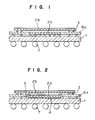
- FIG. 1 is a diagramatical cross-sectional view of the semiconductor device according to a first embodiment of the present invention
- FIG. 2 is a diagramatical cross-sectional view of the semiconductor device according to a second embodiment of the present invention.
- FIG. 3 is a diagramatical cross-sectional view of the semiconductor device according to a third embodiment of the present invention.
- FIG. 4 is a diagramatical cross-sectional view of the semiconductor device according to a fourth embodiment of the present invention.
- FIG. 5 is a diagramatical cross-sectional view of the semiconductor device according to a fifth embodiment of the present invention.
- FIG. 6 is a diagramatical cross-sectional view of the semiconductor device according to a sixth embodiment of the present invention.
- FIGS. 1 to 6 wherein the same reference numerals designate the same or corresponding parts.
- FIG. 1 A first embodiment of the present invention will be described with reference to FIG. 1 .
- a wiring substrate 1 has a circuit pattern.
- a semiconductor chip 2 a having a surface on which bumps 3 are arranged is connected to the circuit pattern of the wiring substrate 1 by flip-chip bonding.
- a first surrounding substrate 6 a has an opening at its central portion, wherein the opening is sufficient to accommodate the semiconductor chip 2 a .
- the first surrounding substrate 6 a has a circuit pattern, and bumps 3 are arranged on the surface where the circuit pattern is formed.
- the first surrounding substrate 6 a is connected electrically to the circuit pattern of the wiring substrate 1 by flip-chip bonding wherein the semiconductor chip 2 a , attached onto the wiring substrate 1 , is received in the opening formed in the first surrounding substrate 6 a.
- a second semiconductor chip 2 b having a surface on which bumps 3 are arranged is placed on the first surrounding substrate 6 a and is connected to the circuit pattern of the first surrounding substrate 6 a by flip-chip bonding.
- the second semiconductor chip 2 b is adapted to connect electrically the circuit pattern of the wiring substrate 1 through the circuit pattern of the first surrounding substrate 6 a .
- external terminals 7 such as solder balls are formed for external connection on a rear surface of the wiring substrate 1 .
- the first semiconductor chip 2 a and the first surrounding substrate 6 a surrounding the first semiconductor chip 2 a are connected to the wiring substrate 1
- the second semiconductor chip 2 b is connected to the wiring substrate 1 through the first surrounding substrate 6 a . Accordingly, memory chips having different memory capacities can be included in the same and single package, and semiconductor devices having a variety of memory capacities can easily be manufactured. This is because the semiconductor chips 2 a 2 b can respectively be connected easily to the wiring substrate 1 by using the first surrounding substrate 6 a.
- Embodiment 1 a case that the second semiconductor chip 2 b is electrically connected to the circuit pattern of the wiring substrate 1 through the circuit pattern of the first surrounding substrate 6 a is described. However, the same effect as in this embodiment can be achieved even by connecting the semiconductor chip 2 a to the semiconductor chip 2 b through the circuit pattern of the first surrounding substrate 6 a.
- the number of semiconductor chips may be increased by increasing the number of the first surrounding substrate 6 a each receiving therein a semiconductor chip or chips. In this case too, the same effect is obtainable.
- a wiring substrate 1 has a circuit pattern.
- a first semiconductor chip 2 a is die-bonded to the wiring substrate 1 by using a die-bonding material 4 such as solder or resin, and electrodes of the first semiconductor chip 2 a are connected to the circuit pattern of the wiring substrate 1 with wires 5 .
- a first surrounding substrate 6 a is connected to the wiring substrate 1 by flip-chip bonding, and a second semiconductor chip 2 b is connected to the surrounding substrate 6 a by flip-chip bonding in the same manner as in Embodiment 1.
- the first semiconductor chip 2 a and the first surrounding substrate 6 a surrounding the first semiconductor chip 2 a are connected to the wiring substrate 1
- the second semiconductor chip 2 b is connected to the wiring substrate 1 through the first surrounding substrate 6 a . Accordingly, memory chips having different memory capacities can be included in the same and single package, and semiconductor devices having a variety of memory capacities can easily be manufactured. This is because the semiconductor chips 2 a 2 b can respectively be connected easily to the wiring substrate 1 by using the first surrounding substrate 6 a.
- Embodiment 2 a case that the second semiconductor chip 2 b is electrically connected to the circuit pattern of the wiring substrate 1 through the circuit pattern of the first surrounding substrate 6 a is described. However, the same effect as in this embodiment can be achieved even by connecting the semiconductor chip 2 a to the semiconductor chip 2 b through the circuit patter of the first surrounding substrate 6 a.
- the number of semiconductor chips may be increased by increasing the number of the first surrounding substrate 6 a each receiving therein a semiconductor chip or chips. In this case too, the same effect is obtainable.
- a wiring substrate 1 has a circuit pattern.
- a first semiconductor chip 2 a is die-bonded to the wiring substrate 1 by using a die-bonding material 4 such as solder or resin.
- a first surrounding substrate 6 a has an opening at its central portion, wherein the opening is sufficient to accommodate the semiconductor chip 2 a .
- the first surrounding substrate 6 a has a circuit pattern, and bumps 3 are arrange on the surface where the circuit pattern is formed.
- the first surrounding substrate 6 a is connected to the circuit pattern of the wiring substrate 1 by flip-chip bonding wherein the semiconductor chip 2 a , attached onto the wiring substrate 1 , is received in the opening formed in the first surrounding substrate 6 a .
- electrodes of the first semiconductor chip 2 a are connected to the circuit pattern of the surrounding substrate 6 a with wires 5 , and a second semiconductor chip 2 b is connected to the surrounding substrate 6 a by flip-chip bonding in the same manner as in Embodiment 1.
- the first semiconductor chip 2 a and the first surrounding substrate 6 a surrounding the first semiconductor chip 2 a are connected to the wiring substrate 1
- the second semiconductor chip 2 b is connected to the wiring substrate 1 through the first surrounding substrate 6 a . Accordingly, memory chips having different memory capacities can be included in the same and single package, and semiconductor devices having a variety of memory capacities can easily be manufactured. This is because the semiconductor chips 2 a 2 b can respectively be connected easily to the wiring substrate 1 by using the first surrounding substrate 6 a.
- Embodiment 3 a case that the second semiconductor chip 2 b is electrically connected to the circuit pattern of the wiring substrate 1 through the circuit pattern of the first surrounding substrate 6 a is described. However, the same effect as in this embodiment can be achieved even by connecting the semiconductor chip 2 a to the semiconductor chip 2 b through the circuit patter of the first surrounding substrate 6 a.
- the number of semiconductor chips may be increased by increasing the number of the first surrounding substrate 6 a each receiving therein a semiconductor chip or chips. In this case too, the same effect is obtainable.
- a fourth embodiment of the present invention will be described with reference to FIG. 4 .
- a second surrounding substrate 6 b which comprises a two or more number of substrate elements each having a rectangular shape and smaller dimensions than those of the first surrounding substrate 6 a , is arranged around the first semiconductor chip 2 a .
- the other construction is the same as that of Embodiment 1.
- the fourth embodiment performs the same effect as the first embodiment.
- a fifth embodiment of the present invention will be described with reference to FIG. 5 .
- a second surrounding substrate 6 b which comprises a two or more number of substrate elements each having a rectangular shape and smaller dimensions than those of the first surrounding substrate 6 a , is arranged around the first semiconductor chip 2 a .
- the other construction is the same as that of first embodiment.
- the fourth embodiment performs the same effect as the first embodiment.
- a sixth embodiment of the present invention will be described with reference to FIG. 6 .
- a second surrounding substrate 6 b which comprises a two or more number of substrate elements each having a rectangular shape and smaller dimensions than those of the first surrounding substrate 6 a , is arranged around the first semiconductor chip 2 a .
- the other construction is the same as that of first embodiment.
- the fourth embodiment performs the same effect as the first embodiment.
- a first semiconductor chip and a first or second surrounding substrate which surrounds the first semiconductor chip are connected to a wiring substrate, and a second semiconductor chip is connected to the wiring substrate through the first or second surrounding substrate. Accordingly, it is possible to contain memory chips having different memory capacities in a single package whereby a semiconductor device having various memory capacities can easily be obtained.
Abstract
A semiconductor device has a first semiconductor chip 2 a, a wiring substrate 1 connected to the first semiconductor chip 2 a, a first surrounding substrate 6 a which has an opening at a position avoiding the first semiconductor chip 2 a and which is connected onto the wiring substrate 1 by flip-chip bonding, and a second semiconductor chip 2 b connected onto the first surrounding substrate 2 a by flip-chip bonding. A second surrounding substrate 6 b comprising a two or more number of substrate elements is used for the first surrounding substrate 6 a.
Description
1. Field of the Invention
The present invention relates to a packaging structure for a semiconductor device. In particular, it relates to a semiconductor device having reduced outer dimensions and containing a plurality of semiconductor chips.
2. Discussion of Background
A conventional semiconductor device has such a packaging structure that a semiconductor chip is attached onto a wiring substrate by die bonding; the semiconductor chip is connected to the wiring substrate by wire bonding, and the semiconductor chip and wires are covered with a molded resin.
The conventional packaging structure had such a problem that the outer dimensions became large when a plurality of semiconductor chips were to be contained. The present invention aims at solving the abovementioned problem and to provide a semiconductor device capable of reducing the outer dimensions while a plurality of semiconductor chips are contained.
In accordance with a first aspect of the present invention, there is provided a semiconductor device which comprises:
a first semiconductor chip, a wiring substrate connected to the first semiconductor chip, a first surrounding substrate which has an opening at a position avoiding the first semiconductor chip and which is connected onto the wiring substrate by flip-chip bonding, and a second semiconductor chip connected onto the first surrounding substrate by flip-chip bonding.
In accordance with a second aspect of the present invention, there is provided a semiconductor device which comprises:
a first semiconductor chip, a wiring substrate connected to the first semiconductor chip, a second surrounding substrate comprising a two or more number of substrate elements which are arranged around the first semiconductor chip and which are connected onto the wiring substrate by flip-chip bonding, and a second semiconductor chip connected onto the second surrounding substrate by flip-chip bonding.
According to a third aspect of the present invention, there is provided a semiconductor device according to the first or second aspect wherein the first semiconductor chip is electrically connected to the wiring substrate by flip-chip bonding.
According to a fourth aspect of the present invention, there is provided a semiconductor device according to the first or second aspect, wherein the first semiconductor chip is die-bonded to the wiring substrate and is electrically connected to the wiring substrate with wires.
According to a fifth aspect of the present invention, there is provided a semiconductor device according to the first aspect of the invention wherein the first semiconductor chip is die-bonded to the wiring substrate and is connected to the first surrounding substrate with wires.
According to a sixth aspect of the present invention, there is provided a semiconductor device according to the second aspect of the present invention, wherein the first semiconductor chip is die-bonded to the wiring substrate and is connected to the second surrounding substrate with wires.
A more complete appreciation of the invention and many of the attendant advantages thereof will be readily obtained as the same becomes better understood by reference to the following detailed description when considered in connection with the accompanying drawings, wherein:
FIG. 1 is a diagramatical cross-sectional view of the semiconductor device according to a first embodiment of the present invention;
FIG. 2 is a diagramatical cross-sectional view of the semiconductor device according to a second embodiment of the present invention;
FIG. 3 is a diagramatical cross-sectional view of the semiconductor device according to a third embodiment of the present invention;
FIG. 4 is a diagramatical cross-sectional view of the semiconductor device according to a fourth embodiment of the present invention;
FIG. 5 is a diagramatical cross-sectional view of the semiconductor device according to a fifth embodiment of the present invention; and
FIG. 6 is a diagramatical cross-sectional view of the semiconductor device according to a sixth embodiment of the present invention.
Preferred embodiments of the present invention will be described in more detail with reference to FIGS. 1 to 6 wherein the same reference numerals designate the same or corresponding parts.
A first embodiment of the present invention will be described with reference to FIG. 1.
A wiring substrate 1 has a circuit pattern. A semiconductor chip 2 a having a surface on which bumps 3 are arranged is connected to the circuit pattern of the wiring substrate 1 by flip-chip bonding. A first surrounding substrate 6 a has an opening at its central portion, wherein the opening is sufficient to accommodate the semiconductor chip 2 a. The first surrounding substrate 6 a has a circuit pattern, and bumps 3 are arranged on the surface where the circuit pattern is formed. The first surrounding substrate 6 a is connected electrically to the circuit pattern of the wiring substrate 1 by flip-chip bonding wherein the semiconductor chip 2 a, attached onto the wiring substrate 1, is received in the opening formed in the first surrounding substrate 6 a.
Then, a second semiconductor chip 2 b having a surface on which bumps 3 are arranged is placed on the first surrounding substrate 6 a and is connected to the circuit pattern of the first surrounding substrate 6 a by flip-chip bonding. The second semiconductor chip 2 b is adapted to connect electrically the circuit pattern of the wiring substrate 1 through the circuit pattern of the first surrounding substrate 6 a. Then, external terminals 7 such as solder balls are formed for external connection on a rear surface of the wiring substrate 1.
As described above, in the semiconductor device of Embodiment 1, the first semiconductor chip 2 a and the first surrounding substrate 6 a surrounding the first semiconductor chip 2 a are connected to the wiring substrate 1, and the second semiconductor chip 2 b is connected to the wiring substrate 1 through the first surrounding substrate 6 a. Accordingly, memory chips having different memory capacities can be included in the same and single package, and semiconductor devices having a variety of memory capacities can easily be manufactured. This is because the semiconductor chips 2 a 2 b can respectively be connected easily to the wiring substrate 1 by using the first surrounding substrate 6 a.
In Embodiment 1, a case that the second semiconductor chip 2 b is electrically connected to the circuit pattern of the wiring substrate 1 through the circuit pattern of the first surrounding substrate 6 a is described. However, the same effect as in this embodiment can be achieved even by connecting the semiconductor chip 2 a to the semiconductor chip 2 b through the circuit pattern of the first surrounding substrate 6 a.
With respect to Embodiment 1, description has been made as to a case of using a single semiconductor chip received in the opening of the first surrounding substrate 6 a. However, the same effect as in this embodiment can be achieved even by using a plurality of semiconductor chips received in the opening of the first surrounding substrate 6 a.
Further, two semiconductor chips are used in Embodiment 1. However, the number of semiconductor chips may be increased by increasing the number of the first surrounding substrate 6 a each receiving therein a semiconductor chip or chips. In this case too, the same effect is obtainable.
A second embodiment of the present invention will be described with reference to FIG. 2. In FIG. 2, a wiring substrate 1 has a circuit pattern. A first semiconductor chip 2 a is die-bonded to the wiring substrate 1 by using a die-bonding material 4 such as solder or resin, and electrodes of the first semiconductor chip 2 a are connected to the circuit pattern of the wiring substrate 1 with wires 5. Then, a first surrounding substrate 6 a is connected to the wiring substrate 1 by flip-chip bonding, and a second semiconductor chip 2 b is connected to the surrounding substrate 6 a by flip-chip bonding in the same manner as in Embodiment 1.
As described above, in the semiconductor device of Embodiment 2, the first semiconductor chip 2 a and the first surrounding substrate 6 a surrounding the first semiconductor chip 2 a are connected to the wiring substrate 1, and the second semiconductor chip 2 b is connected to the wiring substrate 1 through the first surrounding substrate 6 a. Accordingly, memory chips having different memory capacities can be included in the same and single package, and semiconductor devices having a variety of memory capacities can easily be manufactured. This is because the semiconductor chips 2 a 2 b can respectively be connected easily to the wiring substrate 1 by using the first surrounding substrate 6 a.
In Embodiment 2, a case that the second semiconductor chip 2 b is electrically connected to the circuit pattern of the wiring substrate 1 through the circuit pattern of the first surrounding substrate 6 a is described. However, the same effect as in this embodiment can be achieved even by connecting the semiconductor chip 2 a to the semiconductor chip 2 b through the circuit patter of the first surrounding substrate 6 a.
With respect to Embodiment 2, description has been made as to a case of using a single semiconductor chip received in the opening of the first surrounding substrate 6 a. However, the same effect as in this embodiment can be achieved even by using a plurality of semiconductor chips received in the opening of the first surrounding substrate 6 a.
Further, two semiconductor chips are used in Embodiment 2. However, the number of semiconductor chips may be increased by increasing the number of the first surrounding substrate 6 a each receiving therein a semiconductor chip or chips. In this case too, the same effect is obtainable.
A third embodiment of the present invention will be described with reference to FIG. 3. In FIG. 3, a wiring substrate 1 has a circuit pattern. A first semiconductor chip 2 a is die-bonded to the wiring substrate 1 by using a die-bonding material 4 such as solder or resin. A first surrounding substrate 6 a has an opening at its central portion, wherein the opening is sufficient to accommodate the semiconductor chip 2 a. The first surrounding substrate 6 a has a circuit pattern, and bumps 3 are arrange on the surface where the circuit pattern is formed. The first surrounding substrate 6 a is connected to the circuit pattern of the wiring substrate 1 by flip-chip bonding wherein the semiconductor chip 2 a, attached onto the wiring substrate 1, is received in the opening formed in the first surrounding substrate 6 a. Then, electrodes of the first semiconductor chip 2 a are connected to the circuit pattern of the surrounding substrate 6 a with wires 5, and a second semiconductor chip 2 b is connected to the surrounding substrate 6 a by flip-chip bonding in the same manner as in Embodiment 1.
As described above, in the semiconductor device of Embodiment 3, the first semiconductor chip 2 a and the first surrounding substrate 6 a surrounding the first semiconductor chip 2 a are connected to the wiring substrate 1, and the second semiconductor chip 2 b is connected to the wiring substrate 1 through the first surrounding substrate 6 a. Accordingly, memory chips having different memory capacities can be included in the same and single package, and semiconductor devices having a variety of memory capacities can easily be manufactured. This is because the semiconductor chips 2 a 2 b can respectively be connected easily to the wiring substrate 1 by using the first surrounding substrate 6 a.
In Embodiment 3, a case that the second semiconductor chip 2 b is electrically connected to the circuit pattern of the wiring substrate 1 through the circuit pattern of the first surrounding substrate 6 a is described. However, the same effect as in this embodiment can be achieved even by connecting the semiconductor chip 2 a to the semiconductor chip 2 b through the circuit patter of the first surrounding substrate 6 a.
With respect to Embodiment 3, description has been made as to a case of using a single semiconductor chip received in the opening of the first surrounding substrate 6 a. However, the same effect as in this embodiment can be achieved even by using a plurality of semiconductor chips received in the opening of the first surrounding substrate 6 a.
Further, two semiconductor chips are used in Embodiment 3. However, the number of semiconductor chips may be increased by increasing the number of the first surrounding substrate 6 a each receiving therein a semiconductor chip or chips. In this case too, the same effect is obtainable.
A fourth embodiment of the present invention will be described with reference to FIG. 4. In this embodiment, instead of using the first surrounding substrate 6 a having a larger opening than the semiconductor chip 2 a at its central portion as shown in FIG. 1, a second surrounding substrate 6b which comprises a two or more number of substrate elements each having a rectangular shape and smaller dimensions than those of the first surrounding substrate 6 a, is arranged around the first semiconductor chip 2 a. The other construction is the same as that of Embodiment 1. The fourth embodiment performs the same effect as the first embodiment.
A fifth embodiment of the present invention will be described with reference to FIG. 5. In this embodiment, instead of using the first surrounding substrate 6 a having a larger opening than the semiconductor chip 2 a at its central portion as shown in FIG. 2, a second surrounding substrate 6 b which comprises a two or more number of substrate elements each having a rectangular shape and smaller dimensions than those of the first surrounding substrate 6 a, is arranged around the first semiconductor chip 2 a. The other construction is the same as that of first embodiment. The fourth embodiment performs the same effect as the first embodiment.
A sixth embodiment of the present invention will be described with reference to FIG. 6. In this embodiment, instead of using the first surrounding substrate 6 a having a larger opening than the semiconductor chip 2 a at its central portion as shown in FIG. 3, a second surrounding substrate 6 b which comprises a two or more number of substrate elements each having a rectangular shape and smaller dimensions than those of the first surrounding substrate 6 a, is arranged around the first semiconductor chip 2 a. The other construction is the same as that of first embodiment. The fourth embodiment performs the same effect as the first embodiment.
The inventions having the constructions described above perform the functions and effects as follows.
In the inventions according to the first, second, third, fourth and fifth aspects, a first semiconductor chip and a first or second surrounding substrate which surrounds the first semiconductor chip are connected to a wiring substrate, and a second semiconductor chip is connected to the wiring substrate through the first or second surrounding substrate. Accordingly, it is possible to contain memory chips having different memory capacities in a single package whereby a semiconductor device having various memory capacities can easily be obtained.
Obviously, numerous modifications and variations of the present invention are possible in light of the above teachings. It is therefore to be understood that within the scope of the appended claims, the invention may be practiced otherwise than as specifically described herein.
The entire disclosure of Japanese Patent Application No. 11-334190 filed on Nov. 25, 1999 including specification, claims, drawings and summary are incorporated herein by reference in its entirety.
Claims (8)
1. A semiconductor device which comprises:
a first semiconductor chip,
a wiring substrate connected to the first semiconductor chip,
a first surrounding substrate which has an opening at a position avoiding the first semiconductor chip and which is connected onto the wiring substrate by flip-chip bonding, and
a second semiconductor chip connected onto the first surrounding substrate by flip-chip bonding.
2. The semiconductor device according to claim 1 , wherein the first semiconductor chip is electrically connected to the wiring substrate by flip-chip bonding.
3. The semiconductor device according to claim 1 , wherein the first semiconductor chip is die-bonded to the wiring substrate and is electrically connected to the wiring substrate with wires.
4. The semiconductor device according to claim 1 , wherein the first semiconductor chip is die-bonded to the wiring substrate and is connected to the first surrounding substrate with wires.
5. A semiconductor device which comprises:
a first semiconductor chip,
a wiring substrate connected to the first semiconductor chip,
a second surrounding substrate comprising a two or more number of substrate elements which are arranged around the first semiconductor chip and which are connected onto the wiring substrate by flip-chip bonding, and
a second semiconductor chip connected onto the second surrounding substrate by flip-chip bonding.
6. The semiconductor device according to claim 5 , wherein the first semiconductor chip is electrically connected to the wiring substrate by flip-chip bonding.
7. The semiconductor device according to claim 5 , wherein the first semiconductor chip is die-bonded to the wiring substrate and is electrically connected to the wiring substrate with wires.
8. The semiconductor device according to claim 5 , wherein the first semiconductor chip is die-bonded to the wiring substrate and is connected to the second surrounding substrate with wires.
Applications Claiming Priority (2)
| Application Number | Priority Date | Filing Date | Title |
|---|---|---|---|
| JP33419099A JP2001156251A (en) | 1999-11-25 | 1999-11-25 | Semiconductor device |
| JP11-334190 | 1999-11-25 |
Publications (1)
| Publication Number | Publication Date |
|---|---|
| US6469395B1 true US6469395B1 (en) | 2002-10-22 |
Family
ID=18274558
Family Applications (1)
| Application Number | Title | Priority Date | Filing Date |
|---|---|---|---|
| US09/567,009 Expired - Fee Related US6469395B1 (en) | 1999-11-25 | 2000-05-09 | Semiconductor device |
Country Status (3)
| Country | Link |
|---|---|
| US (1) | US6469395B1 (en) |
| JP (1) | JP2001156251A (en) |
| KR (1) | KR20010049663A (en) |
Cited By (13)
| Publication number | Priority date | Publication date | Assignee | Title |
|---|---|---|---|---|
| US20030047760A1 (en) * | 2001-08-30 | 2003-03-13 | Frank Daeche | Electronic component with at least two semiconductor chips, and process for its production |
| US20030230801A1 (en) * | 2002-06-18 | 2003-12-18 | Tongbi Jiang | Semiconductor device assemblies and packages including multiple semiconductor devices and methods |
| US6746894B2 (en) | 2001-03-30 | 2004-06-08 | Micron Technology, Inc. | Ball grid array interposer, packages and methods |
| US20050046040A1 (en) * | 2003-08-25 | 2005-03-03 | Advanced Semiconductor Engineering, Inc. | Flip chip stacked package |
| US20050218518A1 (en) * | 2002-01-07 | 2005-10-06 | Tongbi Jiang | Semiconductor device assemblies and packages including multiple semiconductor device components |
| US20060072368A1 (en) * | 2004-09-30 | 2006-04-06 | Koh Wei H | High density memory card assembly |
| US20060157843A1 (en) * | 2005-01-17 | 2006-07-20 | Sung-Wook Hwang | Stacked semiconductor package having interposing print circuit board |
| US20070216008A1 (en) * | 2006-03-20 | 2007-09-20 | Gerber Mark A | Low profile semiconductor package-on-package |
| CN100350608C (en) * | 2004-01-09 | 2007-11-21 | 日月光半导体制造股份有限公司 | Multi-chip packaging body |
| WO2008082644A1 (en) * | 2006-12-28 | 2008-07-10 | Spansion Llc | Semiconductor device and method of manufacturing the same |
| US20120001339A1 (en) * | 2010-06-30 | 2012-01-05 | Pramod Malatkar | Bumpless build-up layer package design with an interposer |
| US20130082383A1 (en) * | 2011-10-03 | 2013-04-04 | Texas Instruments Incorporated | Electronic assembly having mixed interface including tsv die |
| US9087765B2 (en) | 2013-03-15 | 2015-07-21 | Qualcomm Incorporated | System-in-package with interposer pitch adapter |
Families Citing this family (2)
| Publication number | Priority date | Publication date | Assignee | Title |
|---|---|---|---|---|
| JP2007081108A (en) * | 2005-09-14 | 2007-03-29 | Yaskawa Electric Corp | Laminated structure of semiconductor chip and semiconductor device using same |
| KR101013617B1 (en) * | 2009-02-06 | 2011-02-10 | 송현석 | Automatic Accounting System of Bus Payment |
Citations (10)
| Publication number | Priority date | Publication date | Assignee | Title |
|---|---|---|---|---|
| JPH05275611A (en) | 1992-03-30 | 1993-10-22 | Nec Corp | Multichip module |
| JPH05326834A (en) | 1992-05-20 | 1993-12-10 | Sumitomo Electric Ind Ltd | High density mounting of integrated circuit chip |
| US5521435A (en) * | 1993-12-13 | 1996-05-28 | Fujitsu Limited | Semiconductor device and a fabrication process thereof |
| US5739581A (en) * | 1995-11-17 | 1998-04-14 | National Semiconductor Corporation | High density integrated circuit package assembly with a heatsink between stacked dies |
| US5783870A (en) * | 1995-03-16 | 1998-07-21 | National Semiconductor Corporation | Method for connecting packages of a stacked ball grid array structure |
| US5808878A (en) * | 1995-03-16 | 1998-09-15 | Kabushiki Kaisha Toshiba | Circuit substrate shielding device |
| EP0892434A2 (en) | 1997-07-18 | 1999-01-20 | Lucent Technologies Inc. | RF IC package |
| US5977640A (en) * | 1998-06-26 | 1999-11-02 | International Business Machines Corporation | Highly integrated chip-on-chip packaging |
| US6028365A (en) * | 1998-03-30 | 2000-02-22 | Micron Technology, Inc. | Integrated circuit package and method of fabrication |
| US6140707A (en) * | 1998-05-07 | 2000-10-31 | 3M Innovative Properties Co. | Laminated integrated circuit package |
-
1999
- 1999-11-25 JP JP33419099A patent/JP2001156251A/en not_active Withdrawn
-
2000
- 2000-05-09 US US09/567,009 patent/US6469395B1/en not_active Expired - Fee Related
- 2000-06-29 KR KR1020000036344A patent/KR20010049663A/en active Search and Examination
Patent Citations (10)
| Publication number | Priority date | Publication date | Assignee | Title |
|---|---|---|---|---|
| JPH05275611A (en) | 1992-03-30 | 1993-10-22 | Nec Corp | Multichip module |
| JPH05326834A (en) | 1992-05-20 | 1993-12-10 | Sumitomo Electric Ind Ltd | High density mounting of integrated circuit chip |
| US5521435A (en) * | 1993-12-13 | 1996-05-28 | Fujitsu Limited | Semiconductor device and a fabrication process thereof |
| US5783870A (en) * | 1995-03-16 | 1998-07-21 | National Semiconductor Corporation | Method for connecting packages of a stacked ball grid array structure |
| US5808878A (en) * | 1995-03-16 | 1998-09-15 | Kabushiki Kaisha Toshiba | Circuit substrate shielding device |
| US5739581A (en) * | 1995-11-17 | 1998-04-14 | National Semiconductor Corporation | High density integrated circuit package assembly with a heatsink between stacked dies |
| EP0892434A2 (en) | 1997-07-18 | 1999-01-20 | Lucent Technologies Inc. | RF IC package |
| US6028365A (en) * | 1998-03-30 | 2000-02-22 | Micron Technology, Inc. | Integrated circuit package and method of fabrication |
| US6140707A (en) * | 1998-05-07 | 2000-10-31 | 3M Innovative Properties Co. | Laminated integrated circuit package |
| US5977640A (en) * | 1998-06-26 | 1999-11-02 | International Business Machines Corporation | Highly integrated chip-on-chip packaging |
Cited By (25)
| Publication number | Priority date | Publication date | Assignee | Title |
|---|---|---|---|---|
| US7528007B2 (en) | 2001-03-30 | 2009-05-05 | Micron Technology, Inc. | Methods for assembling semiconductor devices and interposers |
| US6746894B2 (en) | 2001-03-30 | 2004-06-08 | Micron Technology, Inc. | Ball grid array interposer, packages and methods |
| US20040217459A1 (en) * | 2001-03-30 | 2004-11-04 | Fee Setho Sing | Ball grid array interposer, packages and methods |
| US7274095B2 (en) | 2001-03-30 | 2007-09-25 | Micron Technology, Inc. | Interposers with receptacles for receiving semiconductor devices and assemblies and packages including such interposers |
| US20030047760A1 (en) * | 2001-08-30 | 2003-03-13 | Frank Daeche | Electronic component with at least two semiconductor chips, and process for its production |
| US20050218518A1 (en) * | 2002-01-07 | 2005-10-06 | Tongbi Jiang | Semiconductor device assemblies and packages including multiple semiconductor device components |
| US20030230801A1 (en) * | 2002-06-18 | 2003-12-18 | Tongbi Jiang | Semiconductor device assemblies and packages including multiple semiconductor devices and methods |
| US6906415B2 (en) * | 2002-06-27 | 2005-06-14 | Micron Technology, Inc. | Semiconductor device assemblies and packages including multiple semiconductor devices and methods |
| US7573136B2 (en) * | 2002-06-27 | 2009-08-11 | Micron Technology, Inc. | Semiconductor device assemblies and packages including multiple semiconductor device components |
| US7198980B2 (en) | 2002-06-27 | 2007-04-03 | Micron Technology, Inc. | Methods for assembling multiple semiconductor devices |
| US20040106229A1 (en) * | 2002-06-27 | 2004-06-03 | Tongbi Jiang | Methods for assembling multiple semiconductor devices |
| US20050046040A1 (en) * | 2003-08-25 | 2005-03-03 | Advanced Semiconductor Engineering, Inc. | Flip chip stacked package |
| US7291924B2 (en) * | 2003-08-25 | 2007-11-06 | Advanced Semiconductor Engineering, Inc. | Flip chip stacked package |
| CN100350608C (en) * | 2004-01-09 | 2007-11-21 | 日月光半导体制造股份有限公司 | Multi-chip packaging body |
| US7317250B2 (en) * | 2004-09-30 | 2008-01-08 | Kingston Technology Corporation | High density memory card assembly |
| US20060072368A1 (en) * | 2004-09-30 | 2006-04-06 | Koh Wei H | High density memory card assembly |
| US20060157843A1 (en) * | 2005-01-17 | 2006-07-20 | Sung-Wook Hwang | Stacked semiconductor package having interposing print circuit board |
| US20070216008A1 (en) * | 2006-03-20 | 2007-09-20 | Gerber Mark A | Low profile semiconductor package-on-package |
| WO2008082644A1 (en) * | 2006-12-28 | 2008-07-10 | Spansion Llc | Semiconductor device and method of manufacturing the same |
| US20120001339A1 (en) * | 2010-06-30 | 2012-01-05 | Pramod Malatkar | Bumpless build-up layer package design with an interposer |
| CN102934223A (en) * | 2010-06-30 | 2013-02-13 | 英特尔公司 | Bumpless build-up layer package design with an interposer |
| CN102934223B (en) * | 2010-06-30 | 2016-07-06 | 英特尔公司 | There is the bumpless build up layer encapsulation design of inserting |
| US9818719B2 (en) | 2010-06-30 | 2017-11-14 | Intel Corporation | Bumpless build-up layer package design with an interposer |
| US20130082383A1 (en) * | 2011-10-03 | 2013-04-04 | Texas Instruments Incorporated | Electronic assembly having mixed interface including tsv die |
| US9087765B2 (en) | 2013-03-15 | 2015-07-21 | Qualcomm Incorporated | System-in-package with interposer pitch adapter |
Also Published As
| Publication number | Publication date |
|---|---|
| KR20010049663A (en) | 2001-06-15 |
| JP2001156251A (en) | 2001-06-08 |
Similar Documents
| Publication | Publication Date | Title |
|---|---|---|
| US6882056B2 (en) | Multi-chip package type semiconductor device | |
| US6204562B1 (en) | Wafer-level chip scale package | |
| US5770888A (en) | Integrated chip package with reduced dimensions and leads exposed from the top and bottom of the package | |
| US6982485B1 (en) | Stacking structure for semiconductor chips and a semiconductor package using it | |
| US6781240B2 (en) | Semiconductor package with semiconductor chips stacked therein and method of making the package | |
| US6445077B1 (en) | Semiconductor chip package | |
| US6469395B1 (en) | Semiconductor device | |
| US7202554B1 (en) | Semiconductor package and its manufacturing method | |
| US20080157302A1 (en) | Stacked-package quad flat null lead package | |
| US8264075B2 (en) | Stacked-die package including substrate-ground coupling | |
| US8154111B2 (en) | Near chip size semiconductor package | |
| US20040188818A1 (en) | Multi-chips module package | |
| US20100052118A1 (en) | Micro-layered lead frame semiconductor packages | |
| KR19990024255U (en) | Stacked Ball Grid Array Package | |
| US20070267756A1 (en) | Integrated circuit package and multi-layer lead frame utilized | |
| KR100351922B1 (en) | Semiconductor package amd method of manufacturing the same | |
| KR200272826Y1 (en) | Chip size package | |
| KR100444175B1 (en) | ball grid array of stack chip package | |
| KR100788340B1 (en) | Semiconductor Package | |
| KR100250148B1 (en) | Bga semiconductor package | |
| KR20040013736A (en) | Method of manufacturing semiconductor package | |
| KR19980082181A (en) | Lead-on chip type chip scale semiconductor package structure and manufacturing method | |
| KR19990016941A (en) | Stackable Business Package | |
| JPH01169958A (en) | Semiconductor package | |
| JPH11150134A (en) | Semiconductor device |
Legal Events
| Date | Code | Title | Description |
|---|---|---|---|
| AS | Assignment |
Owner name: MITSUBISHI DENKI KABUSHIKI KAISHA, JAPAN Free format text: ASSIGNMENT OF ASSIGNORS INTEREST;ASSIGNORS:NISHIHARA, TATSUTO;YASUNAGA, MASATOSHI;REEL/FRAME:010800/0707 Effective date: 20000417 |
|
| FEPP | Fee payment procedure |
Free format text: PAYOR NUMBER ASSIGNED (ORIGINAL EVENT CODE: ASPN); ENTITY STATUS OF PATENT OWNER: LARGE ENTITY |
|
| FPAY | Fee payment |
Year of fee payment: 4 |
|
| REMI | Maintenance fee reminder mailed | ||
| LAPS | Lapse for failure to pay maintenance fees | ||
| STCH | Information on status: patent discontinuation |
Free format text: PATENT EXPIRED DUE TO NONPAYMENT OF MAINTENANCE FEES UNDER 37 CFR 1.362 |
|
| FP | Lapsed due to failure to pay maintenance fee |
Effective date: 20101022 |