US6473339B2 - Redundancy architecture for an interleaved memory - Google Patents
Redundancy architecture for an interleaved memory Download PDFInfo
- Publication number
- US6473339B2 US6473339B2 US09/773,272 US77327201A US6473339B2 US 6473339 B2 US6473339 B2 US 6473339B2 US 77327201 A US77327201 A US 77327201A US 6473339 B2 US6473339 B2 US 6473339B2
- Authority
- US
- United States
- Prior art keywords
- semi
- arrays
- pair
- redundancy
- address
- Prior art date
- Legal status (The legal status is an assumption and is not a legal conclusion. Google has not performed a legal analysis and makes no representation as to the accuracy of the status listed.)
- Expired - Lifetime, expires
Links
Images


Classifications
-
- G—PHYSICS
- G11—INFORMATION STORAGE
- G11C—STATIC STORES
- G11C29/00—Checking stores for correct operation ; Subsequent repair; Testing stores during standby or offline operation
- G11C29/70—Masking faults in memories by using spares or by reconfiguring
- G11C29/78—Masking faults in memories by using spares or by reconfiguring using programmable devices
Definitions
- the present invention relates to memory redundancy architectures, and in particular, to an architecture for burst interleaved memories.
- Redundancy is a hardware technique that allows the recovering of eventual defects of a memory array to increase the effective yield of the fabrication process of the device. In most cases, when speaking of redundancy a “column” redundancy is generally intended. Matrix columns containing one or more defects are substituted with spare or redundant columns.
- CAM non-volatile memory units
- Information includes addresses of the location to be repaired, which packet of bit of an addressed word must be replaced, whether or not the bank of the CAM is used to store a failed address, etc.
- redundancy managing architecture The function of a redundancy managing architecture is to verify whether or not the failed addressed location is among the redundant ones, and in case of a positive result, to activate the redundant columns and at the same time to deactivate the decoding of the defective location of the matrix. This must be done for any operation, reading or writing, that implies addressing the defective or failed location.
- the number of CAMs used in a redundancy architecture sets the maximum number of packets (columns, byte, rows . . . ) of the whole array of memory cells that can be redundant or substituted.
- packets columns, byte, rows . . .
- the redundancy architecture is similar to the corresponding decoding structure of the memory matrix.
- the redundancy unit is formed, as depicted in FIG. 1, by a main bit line (MBL) (defined in Metal2), starting from which, four real bit lines (defined in Metal1) that are connected to the drains of the respective redundancy cells, are decoded.
- MBL main bit line
- a first approach is redundancy at the output, i.e., replacement of the single line to which the fail belongs.
- a second approach is redundancy by packets, which is a full or partial substitution of the group of bit lines of the word affected by a fail, as addressed during a reading.
- the redundancy architecture may contemplate the repairing of an 8-bit packet (i.e., of the byte high or of the byte low) of an addressed 16-bit word, irrespectively of the fact that the defect can be verified on a single bit of one of the bytes and not on all the 8-bits.
- the whole array of cells is split in several parts (typically in two semi-arrays EVEN/ODD ) that are singularly addressable to avoid problems in managing two partly time overlapped readings as previously discussed.
- the number of sense amplifiers are equal to the number of outputs.
- the selection of the redundant column and the deselection of the column to be redundant is commonly done by acting on the first decoding level while the other decoding levels of the memory matrix remain active.
- the last decoding level that determines which of the bit lines connect to the MBL itself (FIG. 1) will be the selected one, and is active for both the memory matrix and the redundancy structure.
- the read bus is common to both the memory matrix and the redundancy structure. So when a repaired location is addressed, the matrix local decoding is disabled while the redundancy local decoding is activated. This allows the connection between the redundant physical column and the sensing circuitry.
- redundancy By implementing a redundancy per byte, only the matrix local decoding of the word to which the packet (byte) to be replaced belongs will be deactivated, while the other eight local decodings will still be selecting a matrix location. It is clear that the redundancy, which is essential to guarantee an acceptable yield of the fabrication process, has a cost in terms of silicon area consumption, and therefore, it is of great importance to optimize its performances while minimizing the area dedicated to it.
- the redundancy selection circuitry or the number of banks of CAMs, remains unchanged because nothing else is modified.
- the total number of packets of redundancy columns is simply split, i.e., subdivided into subgroups. This arrangement proves itself extremely advantageous. It simplifies the managing of the redundancy and determines a saving of silicon area.
- the approach of the invention does not impose any restriction despite the fact that it is no longer possible to substitute (redundant) two bytes of a same addressed location (word).
- the condition of independence of redundancy for the banks of subdivision of an interleaved memory is fully accomplished allowing, as already discussed above, the possibility of having redundant successive locations that could be read during the same time interval when accessing the memory in burst mode.
- Another advantage of the subdivision of the redundancy architectures in distinct subgroups includes the fact that in terms of layout, the amplitude of the read and write buses for a memory organized in 16-bit words can be 16 bits only along the whole width of the physical memory array because the buses to which the redundant MBL will be eventually connected will be local and related to a single bank (in the case of an interleaved memory) and to a single read/write path.
- a commonly used technique to save area includes using separately the four right columns and the four left columns of a packet of eight columns, thus dividing in two portions a full packet of redundancy columns.
- a number of banks of non-volatile registers equal to the maximum number of substitutions that must be ensured, defined during the design of the device, associate to each bank of subdivision of the cells of the whole memory array (typically two semi-arrays of an interleaved memory) a number of redundancy packets. This number is equal to a pre-defined number of banks of non-volatile registers (CAM).
- suitable XOR structures and one or more non-volatile registers are used for selecting the semi-array affected by defects.
- One or more structures of non-volatile registers thus selecting the portion of an addressed word must be substituted.
- redundancy resources can be freely assigned to any subdivided bank of the array and in any combination and/or ratio.
- a double XOR structure for generating the HIT signals and a CAM dedicated to the storage of the most significant column address used as a multiplexing signal of the HIT signal towards the correct portion of the array, for example, towards the EVEN bank or towards the ODD bank of a common interleaved memory subdivided in two semi-arrays, are used.
- FIG. 1 shows a packet of redundancy columns composed of a main bit line from which four real bit lines are connected to the drain of respective redundancy memory cells according to the prior art.
- FIG. 2 is a functional block diagram of a non-volatile memory unit (CAM) dedicated to the storage of the most significant column address, and of the related multiplexing circuitry for directing the HIT signal towards the correct portion of the memory array according to the present invention.
- CAM non-volatile memory unit
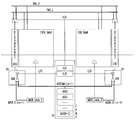
- FIG. 3 is an embodiment of the invention for a burst interleaved memory that is divided into two semi-arrays EVEN and ODD according to the present invention.
- FIG. 4 is a diagram of the redundancy process for the case of a burst interleaved memory according to the present invention.
- the reading (as well as any writing cycle) of a memory location begins with the assigning of an address by the user or by an internal dedicated circuitry.
- the decoding circuitry decodes the assigned address to identify the location of interest and allows either a read or a write operation. If the device has been made redundant during its testing at the end of fabrication, more steps are required to identify the real physical location of the memory.
- the assigned address is XOR combined with the addresses of the redundant locations, and if it corresponds to one of them, a HIT signal is generated that activates the redundancy circuitry substituting the packet of columns containing the failed memory cell with the packet of redundant columns.
- the generated HIT signal is multiplexed in order to replace the correct packet (byte) of the addressed word.
- the redundancy is activated by substituting packets of eight columns, according to the diagram depicted in FIG. 4 .
- the effective activation of the redundancy occurs at the decoding level where the signal HIT 13 lowbyte/HIT 13 highbyte are generated, activates the YMR redundancy decoding, and disables the column decoding in the main semi-array (YM 13 lowbyte/ YM 13 highbyte), as schematically depicted in FIG. 3 .
- the read bus, as well as the Program Load, relative to the failed byte, are connected to the redundant columns corresponding to the columns of the semi-array containing a failed memory cell.
- the use of a double XOR structure to generate the HIT signals and the introduction of a CAM for storing the most significant column address that is used for multiplexing the HIT signals towards the correct semi-arrays ( EVEN or ODD ) guarantees an independent redundancy for the two semi-arrays EVEN/ODD of the (interleaved) memory. This fully satisfies the requirements imposed for the overlap of the readings.
- the managing of the redundancy includes comparing all column addresses with the values stored in the CAMs of the redundancy banks. A logic AND of the single bits of the result of such a comparison produces the HIT signal that, depending on the other essential information (High 13 Byte/Low 13 Byte) stored in another CAM, activates the redundancy circuitry relative to the byte that needs to be substituted.
- n ⁇ 1 column address instead of n, stored in the respective CAMs are used to produce the HIT signal by a logic XOR operation.
- a 0 the most significant address
- the n ⁇ 1 addresses point to two symmetrical locations, one for each semi-arrays EVEN/ODD , while the n ⁇ th address A 0 serves for selecting between the two symmetrical locations.
Abstract
Description
Claims (26)
Applications Claiming Priority (3)
| Application Number | Priority Date | Filing Date | Title |
|---|---|---|---|
| EP00830158.2 | 2000-03-02 | ||
| EP00830158A EP1130517B1 (en) | 2000-03-02 | 2000-03-02 | Redundancy architecture for an interleaved memory |
| EP00830158 | 2000-03-02 |
Publications (2)
| Publication Number | Publication Date |
|---|---|
| US20010026476A1 US20010026476A1 (en) | 2001-10-04 |
| US6473339B2 true US6473339B2 (en) | 2002-10-29 |
Family
ID=8175218
Family Applications (1)
| Application Number | Title | Priority Date | Filing Date |
|---|---|---|---|
| US09/773,272 Expired - Lifetime US6473339B2 (en) | 2000-03-02 | 2001-01-31 | Redundancy architecture for an interleaved memory |
Country Status (3)
| Country | Link |
|---|---|
| US (1) | US6473339B2 (en) |
| EP (1) | EP1130517B1 (en) |
| DE (1) | DE60011035T2 (en) |
Cited By (15)
| Publication number | Priority date | Publication date | Assignee | Title |
|---|---|---|---|---|
| US20030133340A1 (en) * | 2002-01-12 | 2003-07-17 | June Lee | NAND flash memory and method of erasing, programming, and copy-back programming thereof |
| US6618315B2 (en) * | 2001-01-24 | 2003-09-09 | Stmicroelectronics S.R.L. | Non-volatile, electrically alterable semiconductor memory |
| US6665768B1 (en) * | 2000-10-12 | 2003-12-16 | Chipwrights Design, Inc. | Table look-up operation for SIMD processors with interleaved memory systems |
| US6732253B1 (en) | 2000-11-13 | 2004-05-04 | Chipwrights Design, Inc. | Loop handling for single instruction multiple datapath processor architectures |
| US20040090827A1 (en) * | 2002-11-08 | 2004-05-13 | Dahlen Eric J. | Interleaved mirrored memory systems |
| US20040093472A1 (en) * | 2002-11-08 | 2004-05-13 | Dahlen Eric J. | Memory controllers with interleaved mirrored memory modes |
| US6931518B1 (en) | 2000-11-28 | 2005-08-16 | Chipwrights Design, Inc. | Branching around conditional processing if states of all single instruction multiple datapaths are disabled and the computer program is non-deterministic |
| US20100061287A1 (en) * | 2008-09-10 | 2010-03-11 | Samsung Electronics Co., Ltd. | Efficient coding schemes for retransmissions in multicast transmission |
| US7996671B2 (en) | 2003-11-17 | 2011-08-09 | Bluerisc Inc. | Security of program executables and microprocessors based on compiler-architecture interaction |
| US20120069659A1 (en) * | 2008-07-23 | 2012-03-22 | Micron Technology, Inc. | Memory with interleaved read and redundant columns |
| US8607209B2 (en) | 2004-02-04 | 2013-12-10 | Bluerisc Inc. | Energy-focused compiler-assisted branch prediction |
| US8713233B2 (en) | 2010-05-04 | 2014-04-29 | Samsung Electronics Co., Ltd. | Interconnect, bus system with interconnect and bus system operating method |
| US9069938B2 (en) | 2006-11-03 | 2015-06-30 | Bluerisc, Inc. | Securing microprocessors against information leakage and physical tampering |
| US9235393B2 (en) | 2002-07-09 | 2016-01-12 | Iii Holdings 2, Llc | Statically speculative compilation and execution |
| US9569186B2 (en) | 2003-10-29 | 2017-02-14 | Iii Holdings 2, Llc | Energy-focused re-compilation of executables and hardware mechanisms based on compiler-architecture interaction and compiler-inserted control |
Families Citing this family (2)
| Publication number | Priority date | Publication date | Assignee | Title |
|---|---|---|---|---|
| EP1130517B1 (en) * | 2000-03-02 | 2004-05-26 | STMicroelectronics S.r.l. | Redundancy architecture for an interleaved memory |
| US7924638B2 (en) * | 2007-04-18 | 2011-04-12 | Arm Limited | Redundancy architecture for an integrated circuit memory |
Citations (9)
| Publication number | Priority date | Publication date | Assignee | Title |
|---|---|---|---|---|
| EP0561370A2 (en) | 1992-03-19 | 1993-09-22 | Kabushiki Kaisha Toshiba | A clock-synchronous semiconductor memory device and access method thereof |
| US5559990A (en) | 1992-02-14 | 1996-09-24 | Advanced Micro Devices, Inc. | Memories with burst mode access |
| US5596539A (en) | 1995-12-28 | 1997-01-21 | Lsi Logic Corporation | Method and apparatus for a low power self-timed memory control system |
| US5696917A (en) | 1994-06-03 | 1997-12-09 | Intel Corporation | Method and apparatus for performing burst read operations in an asynchronous nonvolatile memory |
| US5831393A (en) * | 1992-03-12 | 1998-11-03 | Emc Corporation | Flexible parity generation circuit |
| US5966724A (en) | 1996-01-11 | 1999-10-12 | Micron Technology, Inc. | Synchronous memory device with dual page and burst mode operations |
| EP0961283A2 (en) | 1998-05-28 | 1999-12-01 | Fujitsu Limited | Memory circuit |
| JP2001236794A (en) * | 2000-02-24 | 2001-08-31 | Hitachi Ltd | Semiconductor storage |
| US20010026476A1 (en) * | 2000-03-02 | 2001-10-04 | Stmicroelectronics S.R.L. | Redundancy architecture for an interleaved memory |
Family Cites Families (1)
| Publication number | Priority date | Publication date | Assignee | Title |
|---|---|---|---|---|
| US5999463A (en) * | 1997-07-21 | 1999-12-07 | Samsung Electronics Co., Ltd. | Redundancy fuse box and semiconductor device including column redundancy fuse box shared by a plurality of memory blocks |
-
2000
- 2000-03-02 EP EP00830158A patent/EP1130517B1/en not_active Expired - Lifetime
- 2000-03-02 DE DE60011035T patent/DE60011035T2/en not_active Expired - Lifetime
-
2001
- 2001-01-31 US US09/773,272 patent/US6473339B2/en not_active Expired - Lifetime
Patent Citations (9)
| Publication number | Priority date | Publication date | Assignee | Title |
|---|---|---|---|---|
| US5559990A (en) | 1992-02-14 | 1996-09-24 | Advanced Micro Devices, Inc. | Memories with burst mode access |
| US5831393A (en) * | 1992-03-12 | 1998-11-03 | Emc Corporation | Flexible parity generation circuit |
| EP0561370A2 (en) | 1992-03-19 | 1993-09-22 | Kabushiki Kaisha Toshiba | A clock-synchronous semiconductor memory device and access method thereof |
| US5696917A (en) | 1994-06-03 | 1997-12-09 | Intel Corporation | Method and apparatus for performing burst read operations in an asynchronous nonvolatile memory |
| US5596539A (en) | 1995-12-28 | 1997-01-21 | Lsi Logic Corporation | Method and apparatus for a low power self-timed memory control system |
| US5966724A (en) | 1996-01-11 | 1999-10-12 | Micron Technology, Inc. | Synchronous memory device with dual page and burst mode operations |
| EP0961283A2 (en) | 1998-05-28 | 1999-12-01 | Fujitsu Limited | Memory circuit |
| JP2001236794A (en) * | 2000-02-24 | 2001-08-31 | Hitachi Ltd | Semiconductor storage |
| US20010026476A1 (en) * | 2000-03-02 | 2001-10-04 | Stmicroelectronics S.R.L. | Redundancy architecture for an interleaved memory |
Cited By (32)
| Publication number | Priority date | Publication date | Assignee | Title |
|---|---|---|---|---|
| US6665768B1 (en) * | 2000-10-12 | 2003-12-16 | Chipwrights Design, Inc. | Table look-up operation for SIMD processors with interleaved memory systems |
| US6732253B1 (en) | 2000-11-13 | 2004-05-04 | Chipwrights Design, Inc. | Loop handling for single instruction multiple datapath processor architectures |
| US20040158691A1 (en) * | 2000-11-13 | 2004-08-12 | Chipwrights Design, Inc., A Massachusetts Corporation | Loop handling for single instruction multiple datapath processor architectures |
| US6931518B1 (en) | 2000-11-28 | 2005-08-16 | Chipwrights Design, Inc. | Branching around conditional processing if states of all single instruction multiple datapaths are disabled and the computer program is non-deterministic |
| US6618315B2 (en) * | 2001-01-24 | 2003-09-09 | Stmicroelectronics S.R.L. | Non-volatile, electrically alterable semiconductor memory |
| US20030133340A1 (en) * | 2002-01-12 | 2003-07-17 | June Lee | NAND flash memory and method of erasing, programming, and copy-back programming thereof |
| US6813184B2 (en) * | 2002-01-12 | 2004-11-02 | Samsung Electronics Co., Ltd. | NAND flash memory and method of erasing, programming, and copy-back programming thereof |
| US10101978B2 (en) | 2002-07-09 | 2018-10-16 | Iii Holdings 2, Llc | Statically speculative compilation and execution |
| US9235393B2 (en) | 2002-07-09 | 2016-01-12 | Iii Holdings 2, Llc | Statically speculative compilation and execution |
| US20040090827A1 (en) * | 2002-11-08 | 2004-05-13 | Dahlen Eric J. | Interleaved mirrored memory systems |
| US7017017B2 (en) | 2002-11-08 | 2006-03-21 | Intel Corporation | Memory controllers with interleaved mirrored memory modes |
| US7076618B2 (en) | 2002-11-08 | 2006-07-11 | Intel Corporation | Memory controllers with interleaved mirrored memory modes |
| US7130229B2 (en) * | 2002-11-08 | 2006-10-31 | Intel Corporation | Interleaved mirrored memory systems |
| US20050262388A1 (en) * | 2002-11-08 | 2005-11-24 | Dahlen Eric J | Memory controllers with interleaved mirrored memory modes |
| US20040093472A1 (en) * | 2002-11-08 | 2004-05-13 | Dahlen Eric J. | Memory controllers with interleaved mirrored memory modes |
| US10248395B2 (en) | 2003-10-29 | 2019-04-02 | Iii Holdings 2, Llc | Energy-focused re-compilation of executables and hardware mechanisms based on compiler-architecture interaction and compiler-inserted control |
| US9569186B2 (en) | 2003-10-29 | 2017-02-14 | Iii Holdings 2, Llc | Energy-focused re-compilation of executables and hardware mechanisms based on compiler-architecture interaction and compiler-inserted control |
| US9582650B2 (en) | 2003-11-17 | 2017-02-28 | Bluerisc, Inc. | Security of program executables and microprocessors based on compiler-architecture interaction |
| US7996671B2 (en) | 2003-11-17 | 2011-08-09 | Bluerisc Inc. | Security of program executables and microprocessors based on compiler-architecture interaction |
| US8607209B2 (en) | 2004-02-04 | 2013-12-10 | Bluerisc Inc. | Energy-focused compiler-assisted branch prediction |
| US9244689B2 (en) | 2004-02-04 | 2016-01-26 | Iii Holdings 2, Llc | Energy-focused compiler-assisted branch prediction |
| US9697000B2 (en) | 2004-02-04 | 2017-07-04 | Iii Holdings 2, Llc | Energy-focused compiler-assisted branch prediction |
| US10268480B2 (en) | 2004-02-04 | 2019-04-23 | Iii Holdings 2, Llc | Energy-focused compiler-assisted branch prediction |
| US9940445B2 (en) | 2006-11-03 | 2018-04-10 | Bluerisc, Inc. | Securing microprocessors against information leakage and physical tampering |
| US9069938B2 (en) | 2006-11-03 | 2015-06-30 | Bluerisc, Inc. | Securing microprocessors against information leakage and physical tampering |
| US10430565B2 (en) | 2006-11-03 | 2019-10-01 | Bluerisc, Inc. | Securing microprocessors against information leakage and physical tampering |
| US11163857B2 (en) | 2006-11-03 | 2021-11-02 | Bluerisc, Inc. | Securing microprocessors against information leakage and physical tampering |
| US8379448B2 (en) * | 2008-07-23 | 2013-02-19 | Micron Technology, Inc. | Memory with interleaved read and redundant columns |
| US20120069659A1 (en) * | 2008-07-23 | 2012-03-22 | Micron Technology, Inc. | Memory with interleaved read and redundant columns |
| US20100061287A1 (en) * | 2008-09-10 | 2010-03-11 | Samsung Electronics Co., Ltd. | Efficient coding schemes for retransmissions in multicast transmission |
| US9122802B2 (en) | 2010-05-04 | 2015-09-01 | Samsung Electronics Co., Ltd. | Interconnect, bus system with interconnect and bus system operating method |
| US8713233B2 (en) | 2010-05-04 | 2014-04-29 | Samsung Electronics Co., Ltd. | Interconnect, bus system with interconnect and bus system operating method |
Also Published As
| Publication number | Publication date |
|---|---|
| DE60011035T2 (en) | 2004-09-16 |
| DE60011035D1 (en) | 2004-07-01 |
| EP1130517A1 (en) | 2001-09-05 |
| US20010026476A1 (en) | 2001-10-04 |
| EP1130517B1 (en) | 2004-05-26 |
Similar Documents
| Publication | Publication Date | Title |
|---|---|---|
| US6473339B2 (en) | Redundancy architecture for an interleaved memory | |
| US5748528A (en) | EEPROM memory device with simultaneous read and write sector capabilities | |
| US7843746B2 (en) | Method and device for redundancy replacement in semiconductor devices using a multiplexer | |
| US6314032B2 (en) | Semiconductor device with flexible redundancy system | |
| JP4062247B2 (en) | Semiconductor memory device | |
| US6922798B2 (en) | Apparatus and methods for providing enhanced redundancy for an on-die cache | |
| US7286399B2 (en) | Dedicated redundancy circuits for different operations in a flash memory device | |
| US6956769B2 (en) | Semiconductor memory device with a flexible redundancy scheme | |
| US6236602B1 (en) | Dynamic configuration of storage arrays | |
| US7505319B2 (en) | Method and apparatus for high efficiency redundancy scheme for multi-segment SRAM | |
| US7373564B2 (en) | Semiconductor memory | |
| JPH0670880B2 (en) | Semiconductor memory device | |
| JP2007517353A (en) | Flexible and area efficient column redundancy for non-volatile memory | |
| KR20020092829A (en) | Semiconductor memory device | |
| KR100448429B1 (en) | Semiconductor memory device and method for its test | |
| JPH0822698A (en) | Redundant register programming method and column redundant integrated circuit | |
| EP0689695A1 (en) | Fault tolerant memory system | |
| US6310805B1 (en) | Architecture for a dual-bank page mode memory with redundancy | |
| US20040015667A1 (en) | System and method for providing one-time programmable memory with fault tolerance | |
| CN101563675A (en) | A new implementation of column redundancy for a flash memory with a high write parallelism | |
| JP2003122638A (en) | Semiconductor integrated circuit device | |
| US7263011B2 (en) | Memory circuit with flexible bitline-related and/or wordline-related defect memory cell substitution | |
| TW200301483A (en) | Twisted bit-line compensation for dram having redundancy | |
| US6809972B2 (en) | Circuit technique for column redundancy fuse latches | |
| US6876580B2 (en) | Semiconductor memory device having a burst continuous read function |
Legal Events
| Date | Code | Title | Description |
|---|---|---|---|
| AS | Assignment |
Owner name: STMICROELECTRONICS S.R.L., ITALY Free format text: ASSIGNMENT OF ASSIGNORS INTEREST;ASSIGNORS:DE AMBROGGI, LUCA GIUSEPPE;CAMPANALE, FABRIZIO;NICOSIA, SALVATORE;AND OTHERS;REEL/FRAME:011925/0378 Effective date: 20010321 |
|
| STCF | Information on status: patent grant |
Free format text: PATENTED CASE |
|
| CC | Certificate of correction | ||
| FEPP | Fee payment procedure |
Free format text: PAYOR NUMBER ASSIGNED (ORIGINAL EVENT CODE: ASPN); ENTITY STATUS OF PATENT OWNER: LARGE ENTITY |
|
| FPAY | Fee payment |
Year of fee payment: 4 |
|
| FPAY | Fee payment |
Year of fee payment: 8 |
|
| AS | Assignment |
Owner name: MICRON TECHNOLOGY, INC., IDAHO Free format text: ASSIGNMENT OF ASSIGNORS INTEREST;ASSIGNOR:STMICROELECTRONICS, S.R.L. (FORMERLY KNOWN AS SGS-THMSON MICROELECTRONICS S.R.L.);REEL/FRAME:031796/0348 Effective date: 20120523 |
|
| FPAY | Fee payment |
Year of fee payment: 12 |
|
| AS | Assignment |
Owner name: U.S. BANK NATIONAL ASSOCIATION, AS COLLATERAL AGENT, CALIFORNIA Free format text: SECURITY INTEREST;ASSIGNOR:MICRON TECHNOLOGY, INC.;REEL/FRAME:038669/0001 Effective date: 20160426 Owner name: U.S. BANK NATIONAL ASSOCIATION, AS COLLATERAL AGEN Free format text: SECURITY INTEREST;ASSIGNOR:MICRON TECHNOLOGY, INC.;REEL/FRAME:038669/0001 Effective date: 20160426 |
|
| AS | Assignment |
Owner name: MORGAN STANLEY SENIOR FUNDING, INC., AS COLLATERAL AGENT, MARYLAND Free format text: PATENT SECURITY AGREEMENT;ASSIGNOR:MICRON TECHNOLOGY, INC.;REEL/FRAME:038954/0001 Effective date: 20160426 Owner name: MORGAN STANLEY SENIOR FUNDING, INC., AS COLLATERAL Free format text: PATENT SECURITY AGREEMENT;ASSIGNOR:MICRON TECHNOLOGY, INC.;REEL/FRAME:038954/0001 Effective date: 20160426 |
|
| AS | Assignment |
Owner name: U.S. BANK NATIONAL ASSOCIATION, AS COLLATERAL AGENT, CALIFORNIA Free format text: CORRECTIVE ASSIGNMENT TO CORRECT THE REPLACE ERRONEOUSLY FILED PATENT #7358718 WITH THE CORRECT PATENT #7358178 PREVIOUSLY RECORDED ON REEL 038669 FRAME 0001. ASSIGNOR(S) HEREBY CONFIRMS THE SECURITY INTEREST;ASSIGNOR:MICRON TECHNOLOGY, INC.;REEL/FRAME:043079/0001 Effective date: 20160426 Owner name: U.S. BANK NATIONAL ASSOCIATION, AS COLLATERAL AGEN Free format text: CORRECTIVE ASSIGNMENT TO CORRECT THE REPLACE ERRONEOUSLY FILED PATENT #7358718 WITH THE CORRECT PATENT #7358178 PREVIOUSLY RECORDED ON REEL 038669 FRAME 0001. ASSIGNOR(S) HEREBY CONFIRMS THE SECURITY INTEREST;ASSIGNOR:MICRON TECHNOLOGY, INC.;REEL/FRAME:043079/0001 Effective date: 20160426 |
|
| AS | Assignment |
Owner name: JPMORGAN CHASE BANK, N.A., AS COLLATERAL AGENT, ILLINOIS Free format text: SECURITY INTEREST;ASSIGNORS:MICRON TECHNOLOGY, INC.;MICRON SEMICONDUCTOR PRODUCTS, INC.;REEL/FRAME:047540/0001 Effective date: 20180703 Owner name: JPMORGAN CHASE BANK, N.A., AS COLLATERAL AGENT, IL Free format text: SECURITY INTEREST;ASSIGNORS:MICRON TECHNOLOGY, INC.;MICRON SEMICONDUCTOR PRODUCTS, INC.;REEL/FRAME:047540/0001 Effective date: 20180703 |
|
| AS | Assignment |
Owner name: MICRON TECHNOLOGY, INC., IDAHO Free format text: RELEASE BY SECURED PARTY;ASSIGNOR:U.S. BANK NATIONAL ASSOCIATION, AS COLLATERAL AGENT;REEL/FRAME:047243/0001 Effective date: 20180629 |
|
| AS | Assignment |
Owner name: MICRON TECHNOLOGY, INC., IDAHO Free format text: RELEASE BY SECURED PARTY;ASSIGNOR:MORGAN STANLEY SENIOR FUNDING, INC., AS COLLATERAL AGENT;REEL/FRAME:050937/0001 Effective date: 20190731 |
|
| AS | Assignment |
Owner name: MICRON SEMICONDUCTOR PRODUCTS, INC., IDAHO Free format text: RELEASE BY SECURED PARTY;ASSIGNOR:JPMORGAN CHASE BANK, N.A., AS COLLATERAL AGENT;REEL/FRAME:051028/0001 Effective date: 20190731 Owner name: MICRON TECHNOLOGY, INC., IDAHO Free format text: RELEASE BY SECURED PARTY;ASSIGNOR:JPMORGAN CHASE BANK, N.A., AS COLLATERAL AGENT;REEL/FRAME:051028/0001 Effective date: 20190731 |