US6978343B1 - Error-correcting content addressable memory - Google Patents
Error-correcting content addressable memory Download PDFInfo
- Publication number
- US6978343B1 US6978343B1 US10/213,244 US21324402A US6978343B1 US 6978343 B1 US6978343 B1 US 6978343B1 US 21324402 A US21324402 A US 21324402A US 6978343 B1 US6978343 B1 US 6978343B1
- Authority
- US
- United States
- Prior art keywords
- row
- parity
- value
- cam
- column
- Prior art date
- Legal status (The legal status is an assumption and is not a legal conclusion. Google has not performed a legal analysis and makes no representation as to the accuracy of the status listed.)
- Expired - Lifetime, expires
Links
Images


Classifications
-
- G—PHYSICS
- G11—INFORMATION STORAGE
- G11C—STATIC STORES
- G11C15/00—Digital stores in which information comprising one or more characteristic parts is written into the store and in which information is read-out by searching for one or more of these characteristic parts, i.e. associative or content-addressed stores
-
- G—PHYSICS
- G11—INFORMATION STORAGE
- G11C—STATIC STORES
- G11C29/00—Checking stores for correct operation ; Subsequent repair; Testing stores during standby or offline operation
- G11C29/04—Detection or location of defective memory elements, e.g. cell constructio details, timing of test signals
- G11C2029/0409—Online test
Definitions
- the present invention relates generally to content addressable memory devices, and more particularly to error detection and correction within content addressable memory devices.
- Content addressable memory (CAM) devices are often used in network switching and routing applications to determine forwarding destinations for data packets.
- a CAM device can be instructed to compare a selected portion of an incoming packet, typically a destination field within the packet header, with data values, called CAM words, stored in an associative storage array within the CAM device. If the destination field matches a CAM word, the CAM device records a CAM index that identifies the location of the matching CAM word within the storage array, and asserts a match flag to signal the match. The CAM index is then typically used to index another storage array, either within or separate from the CAM device, to retrieve a destination address or other routing information for the packet.
- CAM arrays As process geometries shrink, the associative storage arrays of CAM devices, i.e., CAM arrays, become increasingly susceptible to errors induced by alpha-particle bombardment. Such errors are commonly referred to as soft errors and may result in false match or mismatch determinations and ultimately in non-delivery of packets or delivery of packets to incorrect destinations. Accordingly it is desirable to provide some technique for detecting and correcting errors within a CAM device.
- a host processor reads the CAM array entry by entry, and compares the array content to an image stored in a backing store (i.e., another memory).
- a backing store i.e., another memory
- an error correction code is stored along with each entry within the CAM array and used to detect and correct errors that occur within the entry.
- error correction codes typically require storage of multiple code bits per storage row, significantly reducing the available data storage space within the CAM array.
- FIG. 1 illustrates a CAM device according to an embodiment of the present invention
- FIG. 2 illustrates an embodiment of the CAM array, read/write circuit and scan controller of FIG. 1 ;
- FIG. 3 illustrates the logical relationship between the contents of the CAM array and row and column parity values
- FIG. 4 illustrates an error scan cycle according to an embodiment of the invention
- FIG. 5 illustrates a CAM array for which row and column parity values are maintained using the error scan cycle described in reference to FIG. 4 ;
- FIGS. 6A–6C illustrate an exemplary error detection and correction operation within the CAM array of FIG. 5 ;
- FIGS. 7A–7C illustrate another exemplary error detection and correction operation within the CAM array of FIG. 5 ;
- FIGS. 8A–8C illustrate another exemplary error detection and correction operation within the CAM array of FIG. 5 ;
- FIG. 9 illustrates an exemplary row of cells within a ternary CAM device
- FIG. 10 illustrates mask read and data read operations that are used to retrieve a row value for parity checking purposes
- FIG. 11 illustrates an embodiment of a row syndrome generator
- FIG. 12 illustrates a write operation in which a column parity word is updated, and a partial column parity word is conditionally updated, by removing the parity contribution of a target row value and applying the parity contribution of a write data value;
- FIG. 13 illustrates an error address register according to an embodiment of the invention
- FIG. 14 illustrates an embodiment of a write driver circuit that includes a driver bank and a row parity generator
- FIG. 15 illustrates a multi-block CAM device according to an embodiment of the invention.
- circuit elements or circuit blocks may be shown or described as multi-conductor or single conductor signal lines.
- Each of the multi-conductor signal lines may alternatively be single-conductor signal lines, and each of the single-conductor signal lines may alternatively be multi-conductor signal lines.
- a signal is said to be “asserted” when the signal is driven to a low or high logic state (or charged to a high logic state or discharged to a low logic state) to indicate a particular condition.
- a signal is said to be “deasserted” to indicate that the signal is driven (or charged or discharged) to a state other than the asserted state (including a high or low logic state, or the floating state that may occur when the signal driving circuit is transitioned to a high impedance condition, such as an open drain or open collector condition).
- a signal driving circuit is said to “output” a signal to a signal receiving circuit when the signal driving circuit asserts (or deasserts, if explicitly stated or indicated by context) the signal on a signal line coupled between the signal driving and signal receiving circuits.
- a signal line is said to be “activated” when a signal is asserted on the signal line, and “deactivated” when the signal is deasserted.
- the prefix symbol “/” attached to signal names indicates that the signal is an active low signal (i.e., the asserted state is a logic low state).
- a line over a signal name e.g., ‘ ⁇ overscore ( ⁇ signal name>) ⁇ ’
- Active low signals may be changed to active high signals and vice-versa as is generally known in the art.
- row and column parity values that correspond to rows and columns of CAM cells within a CAM device are used to detect and automatically correct soft errors.
- a row parity bit is associated with each row of CAM cells
- a column parity bit is associated with each column of CAM cells.
- a scan controller within the CAM device systematically reads each row of CAM cells within a CAM array, generates a parity check bit based on the content of the row (i.e., the row value) and compares the parity check bit against the corresponding row parity bit. If the check bit and the row parity bit do not match, a parity error is signaled and the scan controller stores the address of the row in an error address register.
- each row value is added to a partial column parity word in an excellent-OR operation such that, after all row values have been added, the partial column parity word represents an exclusive-OR combination of the content of all the rows within the CAM array, and each bit within the partial column parity word represents an exclusive-OR of all the bits within a corresponding column of the CAM array.
- the partial column parity word constitutes a newly generated column parity word which may be compared with a previously stored column parity word to detect the presence of a column parity error. If a soft error has occurred within a given cell of the CAM array, the row address of the error (i.e., detected through row parity checking and stored in the error address register), and the bit position of the error (i.e., the column offset of the error detected through column parity checking) constitute row and column error coordinates that uniquely identify the bit in error. Accordingly, the row value containing the bit in error may be read, and the bit in error changed (e.g., complemented) to generate a corrected row value. The corrected row value may then be written back to the CAM array at the error address to clear the error.
- the row address of the error i.e., detected through row parity checking and stored in the error address register
- the bit position of the error i.e., the column offset of the error detected through column parity checking
- the total number of parity bits used to provide error detection and correction is N row parity bits plus M column parity bits, where N is the number of rows of storage to be error corrected, and M is the number of bits per row.
- error correction codes typically require storage of log 2 (M) bits per row such that the total number of error correction code bits to be stored is N*log 2 (M).
- M log 2
- the storage savings grows as the number of rows in the array increases. Note that for other embodiments, each row of storage in the CAM array may use more than one row parity bit and/or each column of storage in the CAM array may use more than one column parity bit.
- FIG. 1 illustrates a CAM device 100 according to an embodiment of the present invention.
- the CAM device includes a CAM array 101 , address circuit 103 , instruction decoder 105 , scan controller 107 , flag circuit 112 , priority encoder 114 , comparand register 115 and read/write circuit 161 .
- Instructions, addresses and comparands are received in the CAM device 100 via interfaces to an instruction bus (IBUS) 145 , address bus (ABUS) 141 and comparand bus (CBUS) 143 , respectively.
- IBUS instruction bus
- ABUS address bus
- CBUS comparand bus
- Each of the buses is preferably a multi-conductor signal path coupled to at least one host device, such as a general purpose processor, digital signal processor, network processor, application specific integrated circuit (ASIC) or other instruction issuing device.
- host device such as a general purpose processor, digital signal processor, network processor, application specific integrated circuit (ASIC) or other instruction issuing device.
- ASIC application specific integrated circuit
- one or more of the buses may be eliminated and the corresponding signals time-multiplexed onto another of the buses.
- the CAM array 101 includes a plurality of CAM cells arranged in rows for storing CAM words.
- each row of CAM cells includes at least one validity cell to store a value that indicates whether the row contains a valid CAM word.
- Each such value is referred to herein as a validity bit, though more than one bit may be used to indicate whether a given row of CAM cells contains a valid entry. Also, additional bits may be stored within each row to enable per-row control of search and row access operations.
- the CAM array 101 is coupled to (i.e., connected directly to or through one or more intervening circuits) the address circuit 103 , priority encoder 114 , flag circuit 112 , comparand register 115 , and read/write circuit 161 .
- the comparand register 115 is used to store a comparand received via the comparand bus 143 , and outputs respective bits of the comparand value onto corresponding comparand lines of the CAM array 101 .
- the comparand register 115 may be omitted and the comparand applied directly to comparand lines from the comparand bus 143 .
- the comparand may be masked by a global mask value (not shown), then compared simultaneously with all the CAM words stored in the CAM array 101 .
- Each of the rows of CAM cells is coupled to a corresponding match line 182 , and any match between the comparand and a valid CAM word results in the corresponding match line 182 being driven (or left charged or discharged) to a match state to signal the match condition to the priority encoder 114 and flag circuit 112 .
- each validity bit that indicates an empty condition i.e., no valid value stored in the row
- prevents a match from being signaled on the corresponding match line for example, by discharging the match line or otherwise driving the match line to a mismatch state.
- the priority encoder 114 determines a highest priority one of the match signals and outputs a corresponding CAM index 174 (i.e., address of the CAM word that generated the highest priority match signal).
- the flag circuit 112 also receives the match signals on match lines 182 , and asserts a match flag 176 (i.e., a match signal) to indicate that a match has been detected. If more than one match is signaled on match lines 182 , the flag circuit 112 may additionally assert a multiple-match flag to indicate that multiple matches have been detected.
- the instruction decoder 105 includes decode circuitry to decode incoming instructions, and control circuitry to respond to the decoded instructions by issuing control and timing signals to other circuit blocks within the CAM device 100 .
- the instruction decoder 105 may be implemented, for example, by a state machine that transitions from state to state in response to transitions of a clock signal (not shown), and incoming instructions and signals received from other circuit blocks within the CAM device 100 .
- the instruction decoder 105 is a lookup table or read only memory (ROM).
- the instruction decoder 105 outputs a select signal 118 (SEL) to the address circuit to select a read or write address source. Addresses may be supplied, for example, from the address bus 141 , the scan controller 107 or from other registers within the CAM device (e.g., next free address register which contains an address of an empty row within the CAM array, a highest priority match register which contains an address of a row within the CAM array that yielded a highest priority match with a comparand value, etc.).
- the address circuit 103 receives an address from the selected address source and decodes the address to activate a corresponding word line 181 . Each word line 181 is coupled to a corresponding row of CAM cells within the CAM array 101 and, when activated, enables a CAM word to be read from or written to the row.
- the scan controller 107 is provided to detect and correct errors in the CAM array 101 under control of the instruction decoder 105 .
- the scan controller 107 outputs a predetermined sequence of scan addresses to the address circuit 103 to systematically read rows of the CAM array 101 for error detection purposes; an operation referred to herein as error scanning.
- the instruction decoder 105 may suspend error scanning from time to time, for example, to execute a host-requested write or read access to the CAM array 101 .
- the instruction decoder 105 outputs one or more control signals 135 (CTL) to the scan controller 107 to selectively enable and disable error scanning, and to notify the scan controller 107 when a write access to the CAM array is to be performed.
- CTL control signals 135
- the scan controller 107 is additionally coupled to the address circuit 103 and read/write circuit 161 . During error scanning, the scan controller 107 outputs a systematic sequence of scan addresses (SA) to the address circuit 103 via path 144 .
- SA systematic sequence of scan addresses
- the select signal 118 from the instruction decoder 105 selects the scan controller 107 as the address source, and each scan address is decoded by the address circuit 103 to activate a corresponding one of the word lines 181 .
- the read/write circuit is set to a read mode by the instruction decoder 105 and senses the row value within the scan-address-selected row of the CAM array 101 (i.e., the row of CAM cells coupled to the activated word line).
- the row value is output by the read/write circuit 161 to the scan controller 107 which checks for a row parity error and updates the column parity calculation.
- the scan controller 107 asserts an error signal 132 (EFLAG) and outputs the scan address as an error address (EADDR).
- ELAG error signal 132
- EADDR error address
- the error signal 132 and error address 131 may be recorded in a device status register, output to another device (e.g., network processor or host processor), or used for other purposes.
- the error address 131 may be compared with each search-generated index 174 to determine whether the index has resulted from a match between the comparand and a corrupted CAM word.
- the scan controller 107 is coupled to a write driver bank within the read/write circuit 161 to enable a corrected row value to be written back to the CAM array at the completion of an error scan cycle. This operation is discussed below in greater detail.
- FIG. 2 illustrates exemplary embodiments of the CAM array 101 , read write circuit 161 and scan controller 107 of FIG. 1 .
- the CAM array 101 includes a plurality of CAM cells 201 arranged in rows and columns. Each row of the CAM cells 201 is coupled to a respective word line 181 and match line 182 , and each column of CAM cells is coupled to a respective pair of comparand lines 184 and 185 (CL and /CL) and bit lines 186 and 187 (BL and /BL). During a compare operation, comparand data is driven differentially onto the pairs of comparand lines so that the CAM cells within a given column each receive complementary signals that correspond to a bit of the comparand.
- each CAM cell 201 includes a compare circuit, data storage element and, optionally, a mask storage element (e.g., for a ternary CAM cell).
- the compare circuit compares the incoming comparand bit to a value stored in the data storage element and affects the state of the corresponding match line 182 according to whether the comparand bit matches the stored value.
- each of the match lines 182 is initially pulled up to a logic high level to indicate a match condition.
- each match line 182 is pulled low (i.e., discharged) by any CAM cells coupled to the match line that detect a mismatch condition.
- This arrangement constitutes a NOR-based CAM array.
- other types of CAM arrays such as NAND-based CAM arrays, may be used.
- each of the CAM cells 201 includes a mask storage element to store a mask bit.
- the mask bit is supplied to the comparator circuit to selectively mask (i.e., according to the state of the mask bit) the detection of a mismatch condition or at least prevent the CAM cell 201 from affecting the state of the match line 182 .
- the mask values stored within a row of CAM cells form a CAM word referred to herein as a mask word.
- the mask word may be treated as a separate dedicated row for parity checking purposes, or as a logical extension of the data word stored within the data storage elements.
- the CAM array 101 also includes a column of validity cells 202 and a column of row parity cells 203 .
- the validity cells 202 operate in generally the same manner as the CAM cells 201 to compare a stored validity bit with a validity-check bit applied on comparand lines 184 and 185 (CL and /CL) and to affect the state of the match line 182 for the corresponding row.
- the validity-check bit has a state that corresponds to a valid row entry so that, if the validity-check bit matches the content of a given validity cell 202 , match indication is enabled (or not suppressed) on the corresponding match line.
- a match may be signaled on the match line if the comparand value otherwise matches the contents of the corresponding row of CAM cells 201 . If the validity-check bit does not match the content of a validity cell, match indication is disabled on the corresponding match line, thereby preventing false match indications that might otherwise result from comparison of a comparand and invalid CMA word.
- the comparand lines coupled to the column of validity cells may be driven by predetermined voltage sources (e.g., a supply voltage and ground voltage) rather than comparand data.
- a reset line 171 is provided to reset the validity bit for each row (i.e., to indicate an invalid or empty state within the row) at initialization time.
- the validity cells may be omitted from the CAM array.
- the row parity cells 203 do not participate in compare operations, but rather are storage elements for storing row parity values that reflect the row parity of the corresponding rows of the CAM array 101 .
- row parity equates to a modulo-2 sum of bits stored within a given row of CAM cells and, optionally, the corresponding validity cell. Thus, if a given row contains an odd number of 1's, the row parity value is a 1. If the row contains an even number of 1's, the row parity value is a 0.
- the row parity may be a modulo-2 count of the number of 0's stored within the row such that, if the row contains an odd number of 0's, the row parity value is a 1, and if the row contains an even number of 0's, the row parity value is a 0.
- the row parity value may be generated within the CAM device as part of an array write operation or supplied by a host device as part of a data write request.
- the read/write circuit 161 includes a bank of write drivers 163 for writing to the CAM array 101 , and a bank of sense amplifiers 162 for reading from the CAM array 101 .
- the CAM array 101 includes a plurality of bit line pairs 186 , 187 (BL and /BL) coupled to respective columns of CAM cells 201 within the CAM array 101 .
- the bit lines constitute an access port for storing data in and retrieving data from a selected row of CAM cells (i.e., row of CAM cells coupled to an activated word line).
- a pair of validity bit lines 193 , 194 (VBL and /VBL) are similarly coupled to the column of validity cells 202 , and a pair of parity bit lines 195 , 196 (PBL and /PBL) are coupled to the column of parity cells 203 to enable write and read access to those cells.
- the write driver bank 163 is enabled to drive a CAM word (received, for example, from the comparand bus 143 and which may include data and/or mask information) onto the bit lines ( 186 , 187 ), and a corresponding validity bit and row parity bit onto the validity bit lines ( 193 , 194 ) and parity bit lines ( 195 , 196 ), respectively.
- the overall write data value (i.e., CAM word, validity bit and row parity bit) is then stored within the row of cells coupled to the address-selected (i.e., activated) word line.
- an address-selected row of the CAM array 101 is enabled to output a row value (e.g., CAM word, validity bit, and row parity bit) onto the various bit lines (i.e., 186 , 187 , 193 , 194 , 195 and 196 ).
- the sense amplifier bank 162 senses and amplifies the row value, and outputs the row value, for example, to the comparand bus 143 and to the scan controller 107 .
- the scan controller 107 includes scan control logic 221 , scan address sequencer 225 , error address register 223 , column parity register 237 , column parity checker 235 , row parity checker 229 and row correction circuit 231 .
- the scan control logic 221 is a state machine that responds to enable and read/write signals from an instruction decoder to carry out error scanning and correction operations.
- the scan address sequencer 225 maintains a scan address value and increments the scan address through a systemic scan sequence in response to an increment signal from the scan control logic 221 . In one embodiment, the scan address is incremented by one from the lowest address to the highest address of the CAM array.
- the scan address may be incremented by amounts other than one (including a negative amount to achieve a down count) and the scan sequence may be started or ended at addresses other than the lowest and highest address.
- the scan address sequencer 225 reaches a final address in the scan sequence, the error scan cycle is concluded and the scan address is reset (or rolls over) to a starting address within the sequence.
- the corresponding row value is read from the CAM array by the read/write circuit 161 and input to the row parity checker 229 .
- the row parity checker 229 generates a row parity-check value, compares the row parity-check value with the stored parity value for the row (i.e., the row parity value read from the row parity cell 203 ), and signals a row parity error to the scan control logic 221 if the generated and stored row parity values do not match.
- the row parity checker 229 includes a bank of exclusive-OR gates to generate the row-parity check value (e.g., by modulo-2 summation of all the bits within the row value), and an exclusive-OR gate to generate a row parity error indicator by modulo-2 summation of the row parity-check value and the row value.
- the modulo-2 sum (i.e., exclusive-OR combination) of the row parity-check value and the row parity value will be nonzero in the event of a single bit error (or an odd number of bit errors) within the row and zero if there are no bit errors (or possibly multiple bit errors that yield the same modulo-2 sum as in the absence of bit errors).
- a type of row parity error indicator referred to herein as a row syndrome (RSYND) is generated; the row syndrome being nonzero in the event of a parity error and zero in absence of a parity error.
- the row syndrome is supplied to the scan control logic 221 .
- the scan control logic 221 If the row syndrome indicates an error (e.g., RSYND is high), the scan control logic 221 outputs a load signal (LDE) to the error address register 223 to enable the scan address from the scan address sequencer 225 to be loaded into the error address register 223 , and outputs a load signal (LDR) to the row correction circuit 231 to store the corrupted row value in a row correction register within the row correction circuit.
- the corrected row value may be read in a second read operation from the CAM array 101 instead of being stored in the row correction register.
- the scan control logic 221 also increments an internally maintained count value in response to the row parity error indication to keep track of the number of row parity errors detected during a given error scan cycle.
- the number of row parity errors detected during an error scan cycle is determined by the number of entries in the error address register 223 .
- each row value read during an error scan cycle is input to the column parity checker 235 where it is included in a running column parity word calculation.
- the column parity checker 235 includes a partial column parity register to store the partial column parity word (i.e., intermediate sum of row values), and a bank of exclusive-OR gates to update the partial column parity word in response to each incoming row value.
- the partial column parity word is zeroed at the beginning of each error scan cycle, then exclusive-ORred with each incoming row value in succession by the bank of exclusive-OR gates. The application of each incoming row value to the column parity word calculation yields an updated partial column parity word which is loaded into the partial column parity register, overwriting the previous value.
- the resulting partial column parity word constitutes a newly generated column parity word which is compared with the previously generated column parity word stored within the column parity register 237 . If the newly generated column parity word does not match the previously stored column parity word, the column parity checks 235 outputs a column parity error signal (CPE) to the scan control logic 221 to signal an error condition.
- the column parity checker generates a column syndrome value (CSYND) by exclusive-ORing the generated and stored column parity values and outputs the column syndrome to the row correction circuit 231 .
- the row correction circuit 231 combines the column syndrome value with the corrupted row value (i.e., stored in the row correction register) in an exclusive-OR operation to generate a corrected row value.
- the corrected row value is output to a mutliplexer 227 which, during a row correction operation, selects the corrected row value to be a write data value.
- the error address register 223 is selected (e.g., by the address circuit 103 of FIG. 1 ) to source the write address during the row correction operation so that the corrected row value is written to the row address from which the corrupted row value was read.
- FIG. 3 illustrates the logical relationship between the contents of the CAM array 101 and the row and column parity values.
- the CAM array 101 includes N rows and M columns, and each CAM cell has a unique row and column coordinate (i, j). Accordingly, the data value (or mask value) at a given location within the CAM array may be expressed as D i,j , and the row and column parity values that correspond to the data value may be expressed as RP i and CP j , respectively.
- the column parity word that includes the column parity values as constituent bits may be generated by reading each row value in succession and exclusive-ORing the row value with a running total. That is:
- CP[M: 1 ] RV[N] ⁇ RV[N- 1 ] ⁇ . . . ⁇ RV[ 1 ], where RV is a given row value and each exclusive-OR operation is a bit-wise exclusive-OR operation between the respective data values within the rows. That is:
- RV[i] ⁇ RV[i- 1 ] D[i, M] ⁇ D[i- 1 ,M], D[i, M- 1 ] ⁇ D[i- 1 ,M- 1 ], . . . , D[i, 1 ] ⁇ D[i- 1 , 1 ]
- different types of parity calculations may be used in alternative embodiments.
- FIG. 4 illustrates an error scan cycle according to one embodiment.
- the partial column parity word (PCP) maintained within the column parity checker 235 of FIG. 2 is reset to zero; the scan address (SA) is reset to the starting address of the scan sequence, and an error count value (ECNT) maintained within the scan control logic 221 of FIG. 2 is reset to zero.
- a row value (RVAL) is read from the CAM array at the scan address.
- the partial column parity word is exclusive-ORed with the row value to generate an updated partial column parity word.
- a row syndrome is generated by exclusive-ORing the bits of the row value with one another and with the row parity value as described in reference to FIG.
- the row syndrome is nonzero (determined at 283 )
- a row parity error has been detected. Accordingly, at 287 the error count value is incremented to record the row parity error, the scan address is stored within the error address register to mark the row-location of the error, and the corrupted row value is stored within the row correction circuit.
- a row check operation of the error scan cycle is completed. If the scan address is not the final scan address within the scan sequence (i.e., determined at 289 ), the scan address is incremented (or decremented) and a row check operation is performed on the next address in the scan sequence starting at 277 .
- the error count value indicates the number of row errors detected during the sequence of row check cycles, and the partial column parity word constitutes a newly generated column parity word (i.e., generated in the manner described in reference to FIG. 3 ). Accordingly, at 291 , the error count is evaluated to determine whether any row parity errors have been detected. If no row parity errors have been detected, then the newly generated column parity value is stored in the column parity register at 293 and the error scan cycle is completed. Note that storing the newly generated column parity value corrects any soft errors that may have occurred within the column parity register itself.
- the error count is evaluated at 295 to determine whether more than one row parity error has been detected. If more than one row parity error has been detected (i.e., error count greater than one), then more than one bit error has occurred, and a multi-bit error is signaled by the scan controller at 303 , for example, by setting a status value within a status register of the CAM device, and/or outputting an error signal to a processor or other device.
- the error count is determined at 295 not to be greater than one, then a single-bit parity error has occurred and the corrupted row value stored within the row correction circuit and the newly generated column parity word are used to generate a corrected row value. More specifically, at 297 , the newly generated column parity word (PCP) is exclusive-ORed, bit for bit, with the column parity word stored within the column parity register (i.e., the column parity word generated during the previous scan cycle) to generate a column syndrome value (CSYND).
- PCP column parity word
- an exclusive OR combination of the newly generated column parity word and the stored column parity word will yield a column syndrome value in which all the constituent bits are zero except the bit that corresponds to the column that produced the column parity error. Accordingly, at 299 , the column syndrome is exclusive-ORed with the corrupted row value within the row correction circuit to complement the bit in error, restoring the bit to its proper state and thereby generating a corrected row value. At 301 the corrected row value is written to the CAM array at the address indicated by the scan address stored within the error address register, overwriting the corrupted row value.
- a soft error may occur in the row parity cells themselves.
- the read/write circuit e.g., element 161 of FIG. 2
- the read/write circuit generates a row parity value for the corrected row value as part of the write operation in 301 so that the row parity value is overwritten along with the corrected row. Consequently, a row parity error caused by a flipped bit in a row parity cell will be corrected by the write-back at 301 . Note that, when a row parity cell is the source of error and no error has occurred within the CAM cells or validity cells, a row parity error is detected, but no column parity error is detected.
- a zero-valued column syndrome will be generated at 297 and exclusive-ORed with the row value stored within the row correction circuit, thereby yielding the same row value read from the error address, but without the row parity value.
- the row parity value generated during the write operation will overwrite the corrupted row parity value, thereby correcting the source of the row parity error.
- the row parity values themselves may be included in the column parity word calculation, thereby enabling detection of an error within the column of row parity cells and generation of a row-parity-correcting column syndrome value.
- the column syndrome value may then be exclusive-ORed with the row value (including the row parity value) within the row correction circuit to correct an error either in the data/mask/validity portion of the row value or the row parity bit of the row value.
- This embodiment is particularly useful in a CAM device that does not otherwise require row parity generation circuitry in its read/write circuit (e.g., row parity values are provided from an external source during host-requested data write operations).
- FIG. 5 illustrates a CAM array 350 including CAM cells arranged in three rows and three columns and for which row and column parity values are maintained using the error scan cycle described in reference to FIG. 4 .
- a given column of the CAM array may include validity cells rather than CAM cells, and that the values maintained within the CAM cells may contain data or mask values.
- the column parity word is depicted as including only three constituent column parity bits (i.e., corresponding to the three columns of the CAM array), the column parity value may additionally include a column parity bit that corresponds to the column of row parity values.
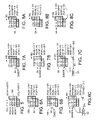
- FIGS. 6A–6C illustrate an exemplary error detection and correction operation within the CAM array 350 accomplished through the error scan cycle described in reference to FIG. 4 .
- an error has occurred in the second column of the second row of the CAM array 350 .
- the bit stored at that location has been flipped from a 1 to a zero, as indicated by the strikethrough and superscript notation.
- the scan address (SA) is presently pointed at the first row of the CAM array such that the row value read from the array (RVAL) is 001; the row syndrome (RSYND) is 0, thus indicating no row parity error in the first row; the error count (ECNT) is zero; and the partial column parity word (PCP) is 001, the result of exclusive-ORing the content of the first row (001) with a reset column parity word (000).
- FIG. 6B depicts the status of the error scan cycle after the scan address has been incremented and a row check operation has been performed on the second row.
- FIG. 6C depicts the status of the error scan cycle after the scan address has been incremented again and a row check operation has been performed on the third row.
- the row value now reflects the content of the third row, 100; the row syndrome is zero, indicating that no row parity error has been detected in the third row; the error count remains at one; and the partial column parity word is now 100, reflecting the overall column parity calculation, 001 ⁇ 001 ⁇ 100.
- the error address remains pointed at row two of the CAM array 350 , and the corrupted value 001 remains present in the row correction register. Because all the row check operations have been completed, the partial column parity word now reflects a newly generated column parity word.
- CSYND column syndrome
- the column syndrome is exclusive-ORed with the content of the row correction register (i.e., the corrupted row value, 001) to generate a corrected row value. 011.
- stores the second row value and the row parity value in the CAM array 350 at the row indicated by the error address At this point the error scan cycle is complete and the CAM array has been restored to an error free condition.
- the error address register is cleared and the parity scan cycle is repeated.
- FIGS. 7A–7C illustrate another exemplary error detection and correction operation within the CAM array 350 accomplished through the error scan cycle described in reference to FIG. 4 .
- an error has occurred within the row parity cell of row one, the correct row parity value, 1, having been flipped to a 0.
- FIG. 7A illustrates the state of scan controller after completion of a row check operation at row one.
- the row value read from the CAM array 350 is 001; the row syndrome is 1, indicating a row parity error; the error count value has been incremented to reflect the row parity error detection; the scan address has been loaded into the error address register such that an error address now points to row one of the CAM array 350 ; the partial column parity word is 001 to reflect the column parity contribution of the row value, and the row correction register has been loaded with the row value for which the parity error was detected.
- FIG. 7B illustrates the state of the scan controller after completion of the row check operation at row two of the CAM array 350 .
- FIG. 7C illustrates the state of the scan controller after completion of the row check operation at row three of the CAM array 350 .
- the row value reflects the content of row three; the row syndrome is zero (no row parity error in row three); the error count and row content register content remain unchanged.
- the scan controller operates in the same manner as in the case of a column parity error; exclusive-ORing the column syndrome with the content of the row correction register to generate a row value to be written back to the CAM array at the error address.
- an additional column parity bit may be included within the column parity word for the column of row parity cells.
- the row parity generator within the read/write circuit is not needed to correct the parity error (and may be omitted if not needed to generate a row parity during a write operation).
- the column syndrome may be applied to the row value (now including the row parity value) within the row correction register to generate a row value and corrected row parity value that may be written back to the CAM array at the error address to clear the row parity error.
- FIGS. 8A–8C illustrate yet another exemplary error detection and correction operation within the CAM array 350 accomplished through the error scan cycle described in reference to FIG. 4 .
- an error has occurred within the column parity word stored in the column parity register; bit three of the column parity word has been flipped from a 0 to a 1.
- FIG. 8A illustrates the state of scan controller after completion of a row check operation at row one.
- FIG. 8A illustrates the state of scan controller after completion of a row check operation at row one.
- the row value read from the CAM array is 001; the row syndrome is 0 (no row parity error); the error count value is zero; and the partial column parity word is 001 to reflect the parity contribution of the row value
- the scan controller state remains substantially unchanged, except that the row value and partial column parity words have been updated according to the row value read from row two. That is, no row parity error is detected within row two, so no error address is loaded into the error address register, no row value is loaded into the row correction register and the error count remains at zero.
- the row syndrome is zero for the third and fourth row operation, so that the error address register and row correction register remain unloaded and the error count remains at zero. Because no row parity error has been detected, no write-back to the CAM array is required to correct a corrupted CAM word. Nevertheless, as shown in FIG. 8C , the stored column parity word is overwritten with the newly generated column parity word, clearing the column parity word error.
- the corrupted column parity word described in reference to FIGS. 8A–8C is corrected without being detected.
- the newly generated column parity word may be exclusive-ORed with the stored column parity word regardless of whether a row parity error was detected, thereby enabling detection of a corrupted column parity word.
- the corruption may then be logged within a status register of the CAM device and/or signaled to a host device to enable tracking of such errors for reliability evaluation, maintenance or other purposes.
- FIG. 9 illustrates an exemplary row 401 of cells within a ternary CAM device in which embodiments of the present invention may be used.
- the row 401 includes N CAM cells 201 N – 201 1 , a validity cell 202 and a parity cell 203 .
- Each of the CAM cells 201 is a ternary CAM cell that includes a data storage element (D), mask storage element (M) and compare circuit (CMP). Though not shown, respective pairs of comparand lines are coupled to the compare circuits to supply comparand data for comparison with the data value within the data storage element.
- D data storage element
- M mask storage element
- CMP compare circuit
- the compare circuit outputs a match or mismatch signal on the match line 182 .
- the validity cell 202 similarly compares a validity bit (stored within validity storage element, V) to a validity-check value to signal validity or invalidity of the match result.
- the match line 182 is precharged to a match indicating condition (e.g., a logic high level) by a precharge circuit 402 .
- the compare circuits within the CAM cells 201 or validity cell 202 may then signal mismatch conditions by pulling the match line 182 low.
- the validity bit itself may be used to affect the state of the match line (e.g., pulling the match line low to prevent a match indication) in an alternative embodiment, obviating the compare circuit (CMP) within the validity cell 202 .
- separate mask and data word lines 181 M (MWL 1 ) and 181 D (DWL i ), respectively, are used to enable read/write access to the data and mask storage elements within the CAM row (e.g., via bit lines 186 and 187 ).
- the parity cell 203 is coupled to the mask word line 181 M and is therefore accessed (i.e., read or written) along with the mask storage elements, while the validity cell 202 is coupled to the data word line 181 D and is accessed along with the data storage elements.
- the word line connections of parity cells 203 and the validity cell 202 may be reversed in alternative embodiments such that the parity cell is accessed with the data storage elements and the validity cell is accessed with the mask storage elements.
- reading a row value from row 401 for parity checking purposes involves two read accesses to the array.
- the row value read operation at block 277 of FIG. 4 is decomposed into a data read at the scan address to retrieve the data bits and validity bit ( 411 ), and a mask read at the scan address to retrieve the mask bits and parity bit ( 413 ).
- the data and mask values may be read in either order or, if additional bit lines are provided to enable simultaneous access to the data and mask storage cells (and the parity and validity cells), the data and mask values may be read concurrently.
- the data and mask components of the row value are concatenated to form the completed row value ( 415 ).
- the concatenation may be achieved by storing the values read at 411 and 413 in respective portions of a row value register or by storing the first value read (mask or data) while the second value read is supplied from the read/write circuit, the first and second values being provided in parallel (i.e., as the row value) to the row correction circuit, row parity checker and column parity checker.
- separate data and mask write operations (which may be carried out concurrently if separate sets of bit lines are provided for access to the data and mask storage elements) are used to write the content of the row correction register to the arrays at the error address indicated by the error address register.
- a shared word line may be used to enable access to both the mask and data storage elements.
- FIG. 11 illustrates an embodiment of a row syndrome generator 420 that may be used to generate a row syndrome value based on values retrieved from the CAM array in separate data and mask reads from a given scan address.
- the row syndrome generator 420 includes a data register 425 to store data and validity bits read in a data read operation, a mask register 427 to store mask and row parity values read in a mask read operation, and a combinatorial logic circuit 428 to generate a modulo-2 sum (i.e., exclusive-OR) of the values within the data and mask registers.
- a modulo-2 sum i.e., exclusive-OR
- each bit of the data register 425 is exclusive-ORed with a corresponding bit from the mask register 427 by a first tier of exclusive-OR gates 429 1 within the logic circuit 428 .
- the output of each exclusive-OR gate within the first tier 429 1 is supplied to a second tier of exclusive-OR gates 429 2 (there being half as many exclusive-OR gates in the second tier as in the first tier), the output of the second tier 429 2 being supplied to a third tier of exclusive-OR gates and so forth to a final exclusive-OR gate 429 X that outputs the row syndrome.
- a nonzero row syndromic indicates a row parity error for the row value.
- the logic circuit 428 may be implemented in alternative embodiments by any circuit (including a different combinatorial logic circuit, or a state machine, look-up table etc.) which generates a row syndrome result according to the above expression.
- a write to the CAM array disrupts the coherency between the CAM array contents and the column parity word.
- the write operation may also disrupt the coherency between the CAM array contents and the partial column parity word, depending on whether the write address (i.e., the address to which the write operation is directed) has already been subjected to a row check operation within the current error scan cycle. In one embodiment, these complications are resolved by aborting the error scan cycle in progress in response to a host-requested a write operation.
- the column parity word is registered based on the updated array contents and the error scan cycle is restarted at the beginning of the scan sequence.
- the error scan cycle in progress is temporarily halted (i.e., suspended) in response to a host-requested write operation, but not aborted.
- the column parity word is updated by removing the parity contribution of the row value to be overwritten (referred to herein as the target row value), and applying the parity contribution of the row value to be written (i.e., the write data).
- the partial column parity word is conditionally updated (i.e., by removing the parity contribution of the target row value to be overwritten and applying the parity contribution of the write data) depending on whether a row check operation has been executed at the write address in the current error scan cycle.
- FIG. 12 illustrates a write operation (WRITE WRVAL@WRITE ADDR) in which the column parity word is updated, and the partial column parity word conditionally is updated, by removing the parity contribution of the target row value and applying the parity contribution of the write data.
- the scan controller is disabled, suspending the current error scan cycle and enabling the read/write port of the CAM array to be used for a host-requested write operation. Referring to the CAM array 101 of FIG.
- an instruction decoder or other control circuit responds to a request to write data by disabling the scan controller 107 (e.g., by deasserting the enable signal, ENABLE) and selecting, via multiplexer 227 , the comparand bus or other data source (e.g., an internal register, a data bus, etc.) a the source of write data.
- the scan controller 107 e.g., by deasserting the enable signal, ENABLE
- the comparand bus or other data source e.g., an internal register, a data bus, etc.
- the instruction decoder may disable the scan controller 107 to enable the read/write port to be used to perform a host-requested read operation or other type of read operation.
- error scanning may be proceed concurrently with host requested read and write operations.
- the target row value is read from the CAM array at the write address.
- the parity contribution of the target entry is removed from the column parity word, for example, by exclusive-ORing the target entry with the column parity word.
- the efficacy of this operation relies upon the associative power of exclusive-OR operations and the fact that a value exclusive-ORed with itself is zero.
- CP a column parity word, CP is formed by A ⁇ B ⁇ C
- the column parity word was generated by exclusive-ORing the target row value with the other row values within the CAM array, exclusive-ORing the target row value with the column parity word efficiency cancels the contribution of the target row value from the column parity word.
- the parity contribution of the write data is applied to the column parity word by exclusive-ORing the write data and the column parity word.
- the write data value and corresponding row parity value are stored in the CAM array at the write address. As described above, the row parity value may be supplied with the write value or generated within the CAM device.
- the stored column parity word reflects the column parity of the updated CAM array but, depending on whether the current error scan cycle has progressed beyond the write address, the partial column parity word may still contain a contribution of the target row value.
- the scan address is compared with the write address to determine whether a row-check operation has been performed at the write address. If the scan address is greater than the write address, then a row check operation has been performed at the write address and the partial column parity word includes a contribution from the target row value. Accordingly, at 513 , the parity contribution of the target row value is removed from the partial column parity word, for example, by exclusive-ORing the target row value with the partial column parity word.
- the parity condition of the write data is applied to the column parity word in an exclusive-OR operation, thereby updating the partial column parity word to reflect the parity of the updated CAM array.
- the scan controller is enabled to continue with the parity scan cycle and the write operation is concluded. Note that the comparison operation at 511 reflects an embodiment in which the scan address is sequenced from low- to high-numbered addresses. Other addresses may be used in alternative embodiments.
- the scan address is compared for equality with the write address at 517 . If the scan address is not equal to the write address, then the scan address has not yet progressed to the write address. Consequently, the target value has not been applied to the calculation of the partial column parity word (and therefore need not be removed) and the write data value, now stored at the write address, will be applied to the partial column parity word in the normal course of the error scan cycle. Accordingly, at 525 the scan controller is enabled to continue the parity scan cycle, and the write operation is concluded.
- the write operation is inspected at 519 to determine whether the write operation is a mask write or a data write (i.e., if the mask data and write data are not written at the same time). If the write operation is a data write operation, the scan controller state is evaluated at 521 to determine how far the current row check operation has progressed. That is, if the error scan cycle was suspended before the data value was read, then the target row value has not been applied to the column parity calculation and the updated data value (i.e., the write value) will be read and applied to the partial column parity word in the normal course when the error-scan cycle is resumed.
- the scan controller state indicates that the data value at the scan address has not yet been read ( 521 )
- the scan controller is re-enabled at 525 and the write operation concluded.
- the operation at 513 and 515 are performed to remove the parity contribution of the data value component of the target row value from the partial column parity word and to apply the parity contribution of the write value to the partial column parity word.
- the scan controller is then re-enabled at 525 and write operation concluded.
- the write operation is determined to be a mask write operation rather than a data write operation
- the parity scan state is evaluated to determine whether the mask value at the scan address has been read. If the mask value has been read, then the operations at 513 and 515 are performed to remove the contribution of the mask value component of the target row value from the partial column parity word, and to apply the parity contribution of the write value to the partial column parity word. The scan controller is then re-enabled at 525 and the write operation concluded.
- the determinations at 519 , 521 and 523 may be simplified to a determination of whether the latter-read of the mask and data values has been read as part of the current row check operation. For example, in an embodiment in which the mask value is read first, and the data value is read second prior to updating the column parity value, then the determinations at 519 , 521 and 523 may be replaced by a single decision block that determines whether the current row check operation has progressed beyond the data read.
- the parity contribution of the portion of the unified row value to be overwritten i.e., the mask or data portion
- the write value contribution added to the portion of the column parity word is removed.
- FIG. 13 illustrates an error address register 223 according to an embodiment of the invention.
- the error address register 223 includes storage for multiple error address entries, each entry including an error address field (EADDR) and a validity field (E).
- the error address field is used to store error addresses (i.e., scan addresses for which a row parity error is signaled), and the validity field is used to store an error bit that indicates whether the corresponding error address field is empty (error bit reset) or loaded with an error address (error bit set).
- the error address register 223 is implemented by a queue circuit having head and tail entries (e.g., a shift register operated as a first-in, first-out circuit).
- a scan address and corresponding error bit is loaded into the tail entry of the queue in response to each assertion of a row parity error indicator 551 (e.g., a signal asserted by the row parity checker 229 of FIG. 2 ).
- the least recently loaded scan address i.e., the oldest error address
- the error address may be stored elsewhere within the CAM device (e.g., a device status register) and/or output as an error signal to another device.
- the error address is also supplied to an address circuit (e.g., circuit 103 of FIG. 1 ) where it is used to address a row of the CAM array during an error correction operation.
- error bits E 0 and E 1 may be input to an AND gate 553 to generate a multi-bit error signal 553 .
- the error signal 132 and the multi-bit error signal 553 may be used within the scan controller to determine the error count (e.g., for the decisions shown at 291 and 295 of FIG. 4 ), obviating storage of a separate error count value.
- the error address register may be a single-entry rather than multi-entry storage.
- the error address register may itself be a CAM (i.e., an error CAM) to permit indices generated during search operations to be compared with error addresses stored within the error address register. Matches between a search-generated index and an error address value within the error address register would indicate that the search-generated index resulted from a match with a corrupted CAM word. Thus, any match signal generated by the error CAM may be used to qualify the corresponding search-generated index.
- FIG. 14 illustrates an embodiment of a write driver circuit 163 that includes a driver bank 571 (e.g., a plurality of differential output drivers to drive differential signals onto the bit lines of the CAM array) and a row parity generator 573 .
- a write data value (WR DATA), which may be a corrected row value, is supplied to the driver bank 307 within the write driver circuit and also to the row parity generator 573 .
- the row parity value is supplied to the driver bank 307 so that the driver bank 571 drives the write data value (optionally including a validity bit) and the row parity value onto bit lines of the CAM array to enable the values to be stored in a word-line-selected row of CAM cells.
- the row parity generator 573 may be omitted from the write driver circuit 163 and the row parity value generated by another source either within or outside the CAM device.
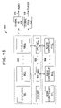
- FIG. 15 illustrates a multi-block CAM device 600 according to an embodiment of the invention.
- the CAM device 600 includes a multi-block CAM array 601 , block-based read/write circuit 605 , block-based scan controller 609 , global priority encoder 625 and global flag circuit 627 .
- the multi-block CAM array 601 includes N CAM blocks 603 1 – 603 N , each of which is independently accessible via a respective read/write circuit 607 1 – 607 N within the block-based read/write circuit 605 .
- Each CAM block 603 is analogous to the CAM array 101 of FIG. 1 and, though not shown in FIG.
- the global priority encoder 625 and global flag circuit 627 are used to generate an overall device index and device flag signals 605 and 606 , based on block-level index and flag signals, respectively.
- the block-based read/write circuit 605 includes a plurality of read/write sub-circuits 607 1 – 607 N to provide and write access to the CAM blocks 603 1 – 603 N , respectively.
- the block-based scan controller 609 similarly includes a plurality of scan sub-controllers 611 1 – 611 N to perform error scanning operations on the CAM blocks 603 1 – 603 N . That is, each scan sub-controller 611 operates generally as described in reference to FIGS. 1–13 to detect row and column parity errors within the corresponding CAM block 603 and to correct such errors by generating corrected row values and writing the corrected values back to the CAM block 603 .
- the CAM device 600 includes a single address circuit (not shown in FIG. 15 ) that is coupled to all the CAM blocks 603 via a common set of word lines.
- a word line is activated during a host requested read or write access, two or more of the CAM blocks may be written to or read from concurrently.
- error scanning in each of the CAM blocks 603 may be carried out concurrently, with the same row of each CAM block being checked during a given row check operation.
- a single scan address sequencer i.e., analogous to element 225 of FIG.
- each CAM block 603 may be provided to generate the sequence of scan addresses rather than including a dedicated address sequencer within each scan sub-controller 611 .
- separate address circuits and word lines are provided for each CAM block 603 to enable concurrent read/write access to two or more of the CAM blocks 603 at different addresses.
- error scanning of the CAM blocks 603 may be carried out independently such that, if error scanning is suspended in a given CAM block 603 (e.g., to execute host-requested access to the CAM block), error scanning may continue in others of the CAM blocks.
- dedicated scan address sequencers may be provided within each of the scan sub-controllers 611 .
- the various embodiments described above can also be adapted to use more than one row parity error bit per row and/or more than one column parity error bit per columns.
- more than one row parity error bit is used per row (e.g., multiple columns of row parity cells each storing row parity bits corresponding to a group of bits in a corresponding row of CAM cells)
- separate scan controllers may be used to process the row parity bits, update the partial column parity word, column parity word and access the CAM cells in the CAM array. Processing of the row parity bits may be performed simultaneously or sequentially.
- a common scan controller may be used and the row parity bits processed in a time-multiplexed manner. Separate variables for the row parity check, row correction, and error count, may be maintained for each column of parity error bits.
- Multiple column parity bits per column of CAM cells may also be used. For example, multiple rows of column parity cells, each for storing column parity bits corresponding to a group of bits in a corresponding column of CAM cells, may be used (e.g., odd and even rows in the CAM array may each have a corresponding column parity word, or any other logical subdivisions or rows within the CAM array).
- separate column parity words are formed by the multiple column bits per row, and each column parity word can be separately maintained by a common scan controller or by a separate scan controllers. The scan controller(s) would update the partial column parity word and column parity words based on whether the scan address indicated that a particular address is within the address space associated with a corresponding column parity word.
- the scan controller(s) can access the corresponding CAM cells in the CAM array either simultaneously or sequentially. Similarly, the scan controller(s) can access the row parity bits simultaneously or sequentially. Note that other embodiments may have multiple column parity words and multiple columns of row parity bits.
Abstract
Description
Claims (43)
Priority Applications (1)
| Application Number | Priority Date | Filing Date | Title |
|---|---|---|---|
| US10/213,244 US6978343B1 (en) | 2002-08-05 | 2002-08-05 | Error-correcting content addressable memory |
Applications Claiming Priority (1)
| Application Number | Priority Date | Filing Date | Title |
|---|---|---|---|
| US10/213,244 US6978343B1 (en) | 2002-08-05 | 2002-08-05 | Error-correcting content addressable memory |
Publications (1)
| Publication Number | Publication Date |
|---|---|
| US6978343B1 true US6978343B1 (en) | 2005-12-20 |
Family
ID=35465721
Family Applications (1)
| Application Number | Title | Priority Date | Filing Date |
|---|---|---|---|
| US10/213,244 Expired - Lifetime US6978343B1 (en) | 2002-08-05 | 2002-08-05 | Error-correcting content addressable memory |
Country Status (1)
| Country | Link |
|---|---|
| US (1) | US6978343B1 (en) |
Cited By (113)
| Publication number | Priority date | Publication date | Assignee | Title |
|---|---|---|---|---|
| US20050060631A1 (en) * | 2003-09-16 | 2005-03-17 | Steven Driediger | Facilitating error detection for content addressable memory |
| US20050289407A1 (en) * | 2004-06-14 | 2005-12-29 | Renesas Technology Corporation | Associative memory capable of searching for data while keeping high data reliability |
| US20060031653A1 (en) * | 2004-08-04 | 2006-02-09 | Emc Corporation | Methods and apparatus for accessing content in a virtual pool on a content addressable storage system |
| US20060123327A1 (en) * | 2002-10-29 | 2006-06-08 | Mosaid Technologies Incorporated | Method and circuit for error correction in CAM cells |
| US20070019455A1 (en) * | 2005-07-25 | 2007-01-25 | Stmicroelectronics, Inc. | Programmable priority encoder |
| US7193876B1 (en) * | 2003-07-15 | 2007-03-20 | Kee Park | Content addressable memory (CAM) arrays having memory cells therein with different susceptibilities to soft errors |
| US20070113158A1 (en) * | 2005-10-28 | 2007-05-17 | Fischer Jeffrey H | High speed CAM lookup using stored encoded key |
| US7305519B1 (en) * | 2004-03-29 | 2007-12-04 | Cisco Technology, Inc. | Error protection for associative memory entries and lookup operations performed thereon |
| US20090172262A1 (en) * | 2007-12-27 | 2009-07-02 | Pliant Technology, Inc. | Metadata rebuild in a flash memory controller following a loss of power |
| US20100050055A1 (en) * | 2008-08-22 | 2010-02-25 | Shingo Tanaka | Data receiving apparatus, data receiving method, and computer-readable recording medium |
| US20100169742A1 (en) * | 2008-12-29 | 2010-07-01 | Texas Instruments Incorporated | Flash memory soft error recovery |
| US7852653B2 (en) * | 2007-06-04 | 2010-12-14 | Hewlett-Packard Development Company, L.P. | Content addressable memory |
| US20110194325A1 (en) * | 2010-02-10 | 2011-08-11 | Ravindraraj Ramaraju | Error detection in a content addressable memory (cam) |
| US20110228601A1 (en) * | 2010-03-17 | 2011-09-22 | Olbrich Aaron K | Mlc self-raid flash data protection scheme |
| US20120117431A1 (en) * | 2009-04-14 | 2012-05-10 | Ben Gurion University Of The Negev | Efficient detection of errors in associative memory |
| US8196017B1 (en) | 2005-01-25 | 2012-06-05 | Netlogic Microsystems, Inc. | Method for on-the-fly error correction in a content addressable memory(CAM) and device therefor |
| US20120198195A1 (en) * | 2011-02-02 | 2012-08-02 | Hewlett-Packard Development Company, L.P. | Data storage system and method |
| US20120311404A1 (en) * | 2011-05-30 | 2012-12-06 | Mikamonu Group Ltd. | Low density parity check decoder |
| US20140108884A1 (en) * | 2012-10-12 | 2014-04-17 | Mediatek Inc. | Method and apparatus for controlling parity check function of content addressable memory device supporting partial write operation |
| US8793543B2 (en) | 2011-11-07 | 2014-07-29 | Sandisk Enterprise Ip Llc | Adaptive read comparison signal generation for memory systems |
| US8891303B1 (en) | 2014-05-30 | 2014-11-18 | Sandisk Technologies Inc. | Method and system for dynamic word line based configuration of a three-dimensional memory device |
| US8910020B2 (en) | 2011-06-19 | 2014-12-09 | Sandisk Enterprise Ip Llc | Intelligent bit recovery for flash memory |
| US8909982B2 (en) | 2011-06-19 | 2014-12-09 | Sandisk Enterprise Ip Llc | System and method for detecting copyback programming problems |
| US8924815B2 (en) | 2011-11-18 | 2014-12-30 | Sandisk Enterprise Ip Llc | Systems, methods and devices for decoding codewords having multiple parity segments |
| US8935590B2 (en) | 2012-10-31 | 2015-01-13 | Infineon Technologies Ag | Circuitry and method for multi-bit correction |
| US8954822B2 (en) | 2011-11-18 | 2015-02-10 | Sandisk Enterprise Ip Llc | Data encoder and decoder using memory-specific parity-check matrix |
| US8990631B1 (en) | 2011-03-03 | 2015-03-24 | Netlogic Microsystems, Inc. | Packet format for error reporting in a content addressable memory |
| US9003264B1 (en) | 2012-12-31 | 2015-04-07 | Sandisk Enterprise Ip Llc | Systems, methods, and devices for multi-dimensional flash RAID data protection |
| US20150098263A1 (en) * | 2013-10-03 | 2015-04-09 | Fujitsu Semiconductor Limited | Ferroelectric memory device |
| US9009576B1 (en) | 2013-03-15 | 2015-04-14 | Sandisk Enterprise Ip Llc | Adaptive LLR based on syndrome weight |
| US20150109840A1 (en) * | 2013-10-21 | 2015-04-23 | SK Hynix Inc. | Semiconductor device and method for operating the same |
| US9043517B1 (en) | 2013-07-25 | 2015-05-26 | Sandisk Enterprise Ip Llc | Multipass programming in buffers implemented in non-volatile data storage systems |
| US9048876B2 (en) | 2011-11-18 | 2015-06-02 | Sandisk Enterprise Ip Llc | Systems, methods and devices for multi-tiered error correction |
| US9070481B1 (en) | 2014-05-30 | 2015-06-30 | Sandisk Technologies Inc. | Internal current measurement for age measurements |
| US9092350B1 (en) | 2013-03-15 | 2015-07-28 | Sandisk Enterprise Ip Llc | Detection and handling of unbalanced errors in interleaved codewords |
| US9092370B2 (en) | 2013-12-03 | 2015-07-28 | Sandisk Enterprise Ip Llc | Power failure tolerant cryptographic erase |
| US9093160B1 (en) | 2014-05-30 | 2015-07-28 | Sandisk Technologies Inc. | Methods and systems for staggered memory operations |
| US9122636B2 (en) | 2013-11-27 | 2015-09-01 | Sandisk Enterprise Ip Llc | Hard power fail architecture |
| US9129665B2 (en) | 2013-12-17 | 2015-09-08 | Sandisk Enterprise Ip Llc | Dynamic brownout adjustment in a storage device |
| US9136877B1 (en) | 2013-03-15 | 2015-09-15 | Sandisk Enterprise Ip Llc | Syndrome layered decoding for LDPC codes |
| US20150261638A1 (en) * | 2014-03-12 | 2015-09-17 | International Business Machines Corporation | Matrix and compression-based error detection |
| US9152555B2 (en) | 2013-11-15 | 2015-10-06 | Sandisk Enterprise IP LLC. | Data management with modular erase in a data storage system |
| US9159437B2 (en) | 2013-06-11 | 2015-10-13 | Sandisk Enterprise IP LLC. | Device and method for resolving an LM flag issue |
| US9158349B2 (en) | 2013-10-04 | 2015-10-13 | Sandisk Enterprise Ip Llc | System and method for heat dissipation |
| US9170941B2 (en) | 2013-04-05 | 2015-10-27 | Sandisk Enterprises IP LLC | Data hardening in a storage system |
| US9214965B2 (en) | 2013-02-20 | 2015-12-15 | Sandisk Enterprise Ip Llc | Method and system for improving data integrity in non-volatile storage |
| US20150381357A1 (en) * | 2014-06-25 | 2015-12-31 | Robert Bosch Gmbh | Method and Apparatus for Generating a Secret Key |
| US9235245B2 (en) | 2013-12-04 | 2016-01-12 | Sandisk Enterprise Ip Llc | Startup performance and power isolation |
| US9235509B1 (en) | 2013-08-26 | 2016-01-12 | Sandisk Enterprise Ip Llc | Write amplification reduction by delaying read access to data written during garbage collection |
| US9236886B1 (en) | 2013-03-15 | 2016-01-12 | Sandisk Enterprise Ip Llc | Universal and reconfigurable QC-LDPC encoder |
| US9239751B1 (en) | 2012-12-27 | 2016-01-19 | Sandisk Enterprise Ip Llc | Compressing data from multiple reads for error control management in memory systems |
| US9244785B2 (en) | 2013-11-13 | 2016-01-26 | Sandisk Enterprise Ip Llc | Simulated power failure and data hardening |
| US9244763B1 (en) | 2013-03-15 | 2016-01-26 | Sandisk Enterprise Ip Llc | System and method for updating a reading threshold voltage based on symbol transition information |
| US9250676B2 (en) | 2013-11-29 | 2016-02-02 | Sandisk Enterprise Ip Llc | Power failure architecture and verification |
| US9263156B2 (en) | 2013-11-07 | 2016-02-16 | Sandisk Enterprise Ip Llc | System and method for adjusting trip points within a storage device |
| US9280429B2 (en) | 2013-11-27 | 2016-03-08 | Sandisk Enterprise Ip Llc | Power fail latching based on monitoring multiple power supply voltages in a storage device |
| US9298608B2 (en) | 2013-10-18 | 2016-03-29 | Sandisk Enterprise Ip Llc | Biasing for wear leveling in storage systems |
| US9323637B2 (en) | 2013-10-07 | 2016-04-26 | Sandisk Enterprise Ip Llc | Power sequencing and data hardening architecture |
| US9329928B2 (en) | 2013-02-20 | 2016-05-03 | Sandisk Enterprise IP LLC. | Bandwidth optimization in a non-volatile memory system |
| US9348377B2 (en) | 2014-03-14 | 2016-05-24 | Sandisk Enterprise Ip Llc | Thermal isolation techniques |
| US9367246B2 (en) | 2013-03-15 | 2016-06-14 | Sandisk Technologies Inc. | Performance optimization of data transfer for soft information generation |
| US9384126B1 (en) | 2013-07-25 | 2016-07-05 | Sandisk Technologies Inc. | Methods and systems to avoid false negative results in bloom filters implemented in non-volatile data storage systems |
| US9390814B2 (en) | 2014-03-19 | 2016-07-12 | Sandisk Technologies Llc | Fault detection and prediction for data storage elements |
| US9390021B2 (en) | 2014-03-31 | 2016-07-12 | Sandisk Technologies Llc | Efficient cache utilization in a tiered data structure |
| US20160217030A1 (en) * | 2015-01-23 | 2016-07-28 | Dong-Min Shin | Memory system and method of operating the memory system |
| US9436831B2 (en) | 2013-10-30 | 2016-09-06 | Sandisk Technologies Llc | Secure erase in a memory device |
| US9442670B2 (en) | 2013-09-03 | 2016-09-13 | Sandisk Technologies Llc | Method and system for rebalancing data stored in flash memory devices |
| US9442662B2 (en) | 2013-10-18 | 2016-09-13 | Sandisk Technologies Llc | Device and method for managing die groups |
| US9443601B2 (en) | 2014-09-08 | 2016-09-13 | Sandisk Technologies Llc | Holdup capacitor energy harvesting |
| US9448876B2 (en) | 2014-03-19 | 2016-09-20 | Sandisk Technologies Llc | Fault detection and prediction in storage devices |
| US9454448B2 (en) | 2014-03-19 | 2016-09-27 | Sandisk Technologies Llc | Fault testing in storage devices |
| US9454420B1 (en) | 2012-12-31 | 2016-09-27 | Sandisk Technologies Llc | Method and system of reading threshold voltage equalization |
| US9485851B2 (en) | 2014-03-14 | 2016-11-01 | Sandisk Technologies Llc | Thermal tube assembly structures |
| US9497889B2 (en) | 2014-02-27 | 2016-11-15 | Sandisk Technologies Llc | Heat dissipation for substrate assemblies |
| US9501398B2 (en) | 2012-12-26 | 2016-11-22 | Sandisk Technologies Llc | Persistent storage device with NVRAM for staging writes |
| US9520197B2 (en) | 2013-11-22 | 2016-12-13 | Sandisk Technologies Llc | Adaptive erase of a storage device |
| US9520162B2 (en) | 2013-11-27 | 2016-12-13 | Sandisk Technologies Llc | DIMM device controller supervisor |
| US9519319B2 (en) | 2014-03-14 | 2016-12-13 | Sandisk Technologies Llc | Self-supporting thermal tube structure for electronic assemblies |
| US9519577B2 (en) | 2013-09-03 | 2016-12-13 | Sandisk Technologies Llc | Method and system for migrating data between flash memory devices |
| US9524235B1 (en) | 2013-07-25 | 2016-12-20 | Sandisk Technologies Llc | Local hash value generation in non-volatile data storage systems |
| US9549457B2 (en) | 2014-02-12 | 2017-01-17 | Sandisk Technologies Llc | System and method for redirecting airflow across an electronic assembly |
| US9582058B2 (en) | 2013-11-29 | 2017-02-28 | Sandisk Technologies Llc | Power inrush management of storage devices |
| US9612948B2 (en) | 2012-12-27 | 2017-04-04 | Sandisk Technologies Llc | Reads and writes between a contiguous data block and noncontiguous sets of logical address blocks in a persistent storage device |
| US9626399B2 (en) | 2014-03-31 | 2017-04-18 | Sandisk Technologies Llc | Conditional updates for reducing frequency of data modification operations |
| US9626400B2 (en) | 2014-03-31 | 2017-04-18 | Sandisk Technologies Llc | Compaction of information in tiered data structure |
| US9639463B1 (en) | 2013-08-26 | 2017-05-02 | Sandisk Technologies Llc | Heuristic aware garbage collection scheme in storage systems |
| US9645749B2 (en) | 2014-05-30 | 2017-05-09 | Sandisk Technologies Llc | Method and system for recharacterizing the storage density of a memory device or a portion thereof |
| US9652381B2 (en) | 2014-06-19 | 2017-05-16 | Sandisk Technologies Llc | Sub-block garbage collection |
| US9697267B2 (en) | 2014-04-03 | 2017-07-04 | Sandisk Technologies Llc | Methods and systems for performing efficient snapshots in tiered data structures |
| US9699263B1 (en) | 2012-08-17 | 2017-07-04 | Sandisk Technologies Llc. | Automatic read and write acceleration of data accessed by virtual machines |
| US9703636B2 (en) | 2014-03-01 | 2017-07-11 | Sandisk Technologies Llc | Firmware reversion trigger and control |
| US9703491B2 (en) | 2014-05-30 | 2017-07-11 | Sandisk Technologies Llc | Using history of unaligned writes to cache data and avoid read-modify-writes in a non-volatile storage device |
| US9703816B2 (en) | 2013-11-19 | 2017-07-11 | Sandisk Technologies Llc | Method and system for forward reference logging in a persistent datastore |
| US20170337015A1 (en) * | 2014-12-05 | 2017-11-23 | Samsung Electronics Co., Ltd. | Memory access control method and apparatus |
| US9870830B1 (en) * | 2013-03-14 | 2018-01-16 | Sandisk Technologies Llc | Optimal multilevel sensing for reading data from a storage medium |
| US10049037B2 (en) | 2013-04-05 | 2018-08-14 | Sandisk Enterprise Ip Llc | Data management in a storage system |
| US10084478B2 (en) * | 2016-05-31 | 2018-09-25 | Arm Limited | Apparatus and method for generating an error code for a block comprising a plurality of data bits and a plurality of address bits |
| US10114557B2 (en) | 2014-05-30 | 2018-10-30 | Sandisk Technologies Llc | Identification of hot regions to enhance performance and endurance of a non-volatile storage device |
| US20180336091A1 (en) * | 2017-05-17 | 2018-11-22 | Unigroup Guoxin Microelectronics Co., Ltd. | Method of Correcting an Error in a Memory Array in a DRAM During a Read Operation and a DRAM |
| US10146448B2 (en) | 2014-05-30 | 2018-12-04 | Sandisk Technologies Llc | Using history of I/O sequences to trigger cached read ahead in a non-volatile storage device |
| US10162748B2 (en) | 2014-05-30 | 2018-12-25 | Sandisk Technologies Llc | Prioritizing garbage collection and block allocation based on I/O history for logical address regions |
| US10216571B2 (en) | 2016-11-10 | 2019-02-26 | Western Digital Technologies, Inc. | System and methodology for error management within a shared non-volatile memory architecture using bloom filters |
| US10254982B2 (en) | 2016-11-10 | 2019-04-09 | Western Digital Technologies, Inc. | System and methodology for low latency error management within a shared non-volatile memory architecture |
| US20190227869A1 (en) * | 2018-01-22 | 2019-07-25 | Micron Technology, Inc. | Enhanced error correcting code capability using variable logical to physical associations of a data block |
| US10372613B2 (en) | 2014-05-30 | 2019-08-06 | Sandisk Technologies Llc | Using sub-region I/O history to cache repeatedly accessed sub-regions in a non-volatile storage device |
| US10439648B1 (en) * | 2018-04-10 | 2019-10-08 | Micron Technology, Inc. | Area efficient implementation of a product code error correcting code decoder |
| US10514867B2 (en) | 2016-11-10 | 2019-12-24 | Western Digital Technologies, Inc. | System and methodology that facilitates error management within a shared non-volatile memory architecture |
| US10656840B2 (en) | 2014-05-30 | 2020-05-19 | Sandisk Technologies Llc | Real-time I/O pattern recognition to enhance performance and endurance of a storage device |
| US10656842B2 (en) | 2014-05-30 | 2020-05-19 | Sandisk Technologies Llc | Using history of I/O sizes and I/O sequences to trigger coalesced writes in a non-volatile storage device |
| US10659082B2 (en) * | 2014-07-18 | 2020-05-19 | Sony Corporation | Receiving device and receiving method |
| US10846175B2 (en) | 2018-04-10 | 2020-11-24 | Micron Technology, Inc. | High throughput bit correction of data inside a word buffer for a product code decoder |
| US10956245B1 (en) * | 2017-07-28 | 2021-03-23 | EMC IP Holding Company LLC | Storage system with host-directed error scanning of solid-state storage devices |
| US20220359033A1 (en) * | 2021-05-04 | 2022-11-10 | Micron Technology, Inc. | Health scan for content addressable memory |
Citations (17)
| Publication number | Priority date | Publication date | Assignee | Title |
|---|---|---|---|---|
| US4112502A (en) | 1976-10-18 | 1978-09-05 | Sperry Rand Corporation | Conditional bypass of error correction for dual memory access time selection |
| US4747080A (en) | 1985-11-12 | 1988-05-24 | Nippon Telegraph & Telephone Corporation | Semiconductor memory having self correction function |
| US5450424A (en) * | 1992-07-27 | 1995-09-12 | Mitsubishi Denki Kabushiki Kaisha | Semiconductor memory device with error checking and correcting function |
| US5491703A (en) | 1992-06-30 | 1996-02-13 | Sgs-Thomson Microelectronics Ltd. | Cam with additional row cells connected to match line |
| US5796758A (en) | 1996-10-08 | 1998-08-18 | International Business Machines Corporation | Self-checking content-addressable memory and method of operation for detecting multiple selected word lines |
| US5872802A (en) | 1996-05-03 | 1999-02-16 | Cypress Semiconductor Corp. | Parity generation and check circuit and method in read data path |
| US5999450A (en) * | 1996-05-09 | 1999-12-07 | Stmicroelectronics S.R.L. | Electrically erasable and programmable non-volatile memory device with testable redundancy circuits |
| US6014755A (en) * | 1992-10-30 | 2000-01-11 | Intel Corporation | Method of managing defects in flash disk memories |
| US6067262A (en) * | 1998-12-11 | 2000-05-23 | Lsi Logic Corporation | Redundancy analysis for embedded memories with built-in self test and built-in self repair |
| US6085334A (en) * | 1998-04-17 | 2000-07-04 | Motorola, Inc. | Method and apparatus for testing an integrated memory device |
| US6154384A (en) | 1999-11-12 | 2000-11-28 | Netlogic Microsystems, Inc. | Ternary content addressable memory cell |
| US6199140B1 (en) | 1997-10-30 | 2001-03-06 | Netlogic Microsystems, Inc. | Multiport content addressable memory device and timing signals |
| US6243281B1 (en) | 2000-06-14 | 2001-06-05 | Netlogic Microsystems, Inc. | Method and apparatus for accessing a segment of CAM cells in an intra-row configurable CAM system |
| US20020083421A1 (en) * | 2000-12-22 | 2002-06-27 | Hitachi America, Ltd. | Assembly language code compilation for an instruction-set architecture containing new instructions using the prior assembler |
| US20020120887A1 (en) * | 2001-02-23 | 2002-08-29 | Hughes Brian William | Cache test sequence for single-ported row repair CAM |
| US6657878B2 (en) * | 2002-02-27 | 2003-12-02 | Integrated Device Technology, Inc. | Content addressable memory (CAM) devices having reliable column redundancy characteristics and methods of operating same |
| US6690595B1 (en) * | 2001-08-03 | 2004-02-10 | Netlogic Microsystems, Inc. | Content addressable memory with selective error logging |
-
2002
- 2002-08-05 US US10/213,244 patent/US6978343B1/en not_active Expired - Lifetime
Patent Citations (17)
| Publication number | Priority date | Publication date | Assignee | Title |
|---|---|---|---|---|
| US4112502A (en) | 1976-10-18 | 1978-09-05 | Sperry Rand Corporation | Conditional bypass of error correction for dual memory access time selection |
| US4747080A (en) | 1985-11-12 | 1988-05-24 | Nippon Telegraph & Telephone Corporation | Semiconductor memory having self correction function |
| US5491703A (en) | 1992-06-30 | 1996-02-13 | Sgs-Thomson Microelectronics Ltd. | Cam with additional row cells connected to match line |
| US5450424A (en) * | 1992-07-27 | 1995-09-12 | Mitsubishi Denki Kabushiki Kaisha | Semiconductor memory device with error checking and correcting function |
| US6014755A (en) * | 1992-10-30 | 2000-01-11 | Intel Corporation | Method of managing defects in flash disk memories |
| US5872802A (en) | 1996-05-03 | 1999-02-16 | Cypress Semiconductor Corp. | Parity generation and check circuit and method in read data path |
| US5999450A (en) * | 1996-05-09 | 1999-12-07 | Stmicroelectronics S.R.L. | Electrically erasable and programmable non-volatile memory device with testable redundancy circuits |
| US5796758A (en) | 1996-10-08 | 1998-08-18 | International Business Machines Corporation | Self-checking content-addressable memory and method of operation for detecting multiple selected word lines |
| US6199140B1 (en) | 1997-10-30 | 2001-03-06 | Netlogic Microsystems, Inc. | Multiport content addressable memory device and timing signals |
| US6085334A (en) * | 1998-04-17 | 2000-07-04 | Motorola, Inc. | Method and apparatus for testing an integrated memory device |
| US6067262A (en) * | 1998-12-11 | 2000-05-23 | Lsi Logic Corporation | Redundancy analysis for embedded memories with built-in self test and built-in self repair |
| US6154384A (en) | 1999-11-12 | 2000-11-28 | Netlogic Microsystems, Inc. | Ternary content addressable memory cell |
| US6243281B1 (en) | 2000-06-14 | 2001-06-05 | Netlogic Microsystems, Inc. | Method and apparatus for accessing a segment of CAM cells in an intra-row configurable CAM system |
| US20020083421A1 (en) * | 2000-12-22 | 2002-06-27 | Hitachi America, Ltd. | Assembly language code compilation for an instruction-set architecture containing new instructions using the prior assembler |
| US20020120887A1 (en) * | 2001-02-23 | 2002-08-29 | Hughes Brian William | Cache test sequence for single-ported row repair CAM |
| US6690595B1 (en) * | 2001-08-03 | 2004-02-10 | Netlogic Microsystems, Inc. | Content addressable memory with selective error logging |
| US6657878B2 (en) * | 2002-02-27 | 2003-12-02 | Integrated Device Technology, Inc. | Content addressable memory (CAM) devices having reliable column redundancy characteristics and methods of operating same |
Non-Patent Citations (2)
| Title |
|---|
| "Error Correction with Hamming Codes," pp. 1-2 downloaded Jun. 22, 2001 from URL http://www.rad.com/networks/1994/err<SUB>-</SUB>con/hamming.htm. |
| John R. Pierce, "Inroduction to Information Theory; Symbols, Signals, and Noise" 2nd Edition, 1980, pp. 145-165, Dover Publications, Inc., ISBN 0-486-24061-4. |
Cited By (162)
| Publication number | Priority date | Publication date | Assignee | Title |
|---|---|---|---|---|
| US7350137B2 (en) * | 2002-10-29 | 2008-03-25 | Mosaid Technologies Incorporated | Method and circuit for error correction in CAM cells |
| US20060123327A1 (en) * | 2002-10-29 | 2006-06-08 | Mosaid Technologies Incorporated | Method and circuit for error correction in CAM cells |
| US7193876B1 (en) * | 2003-07-15 | 2007-03-20 | Kee Park | Content addressable memory (CAM) arrays having memory cells therein with different susceptibilities to soft errors |
| US7296210B2 (en) * | 2003-09-16 | 2007-11-13 | Alcatel-Lucent Inc | Facilitating error detection for content addressable memory |
| US20050060631A1 (en) * | 2003-09-16 | 2005-03-17 | Steven Driediger | Facilitating error detection for content addressable memory |
| US7305519B1 (en) * | 2004-03-29 | 2007-12-04 | Cisco Technology, Inc. | Error protection for associative memory entries and lookup operations performed thereon |
| US7277306B2 (en) * | 2004-06-14 | 2007-10-02 | Renesas Technology Corp. | Associative memory capable of searching for data while keeping high data reliability |
| US20070245168A1 (en) * | 2004-06-14 | 2007-10-18 | Renesas Technology Corporation | Associative memory capable of searching for data while keeping high data reliability |
| US20050289407A1 (en) * | 2004-06-14 | 2005-12-29 | Renesas Technology Corporation | Associative memory capable of searching for data while keeping high data reliability |
| US20060031653A1 (en) * | 2004-08-04 | 2006-02-09 | Emc Corporation | Methods and apparatus for accessing content in a virtual pool on a content addressable storage system |
| US8069269B2 (en) * | 2004-08-04 | 2011-11-29 | Emc Corporation | Methods and apparatus for accessing content in a virtual pool on a content addressable storage system |
| US8196017B1 (en) | 2005-01-25 | 2012-06-05 | Netlogic Microsystems, Inc. | Method for on-the-fly error correction in a content addressable memory(CAM) and device therefor |
| US7196922B2 (en) * | 2005-07-25 | 2007-03-27 | Stmicroelectronics, Inc. | Programmable priority encoder |
| US20070019455A1 (en) * | 2005-07-25 | 2007-01-25 | Stmicroelectronics, Inc. | Programmable priority encoder |
| US20070113158A1 (en) * | 2005-10-28 | 2007-05-17 | Fischer Jeffrey H | High speed CAM lookup using stored encoded key |
| US7761774B2 (en) * | 2005-10-28 | 2010-07-20 | Qualcomm Incorporated | High speed CAM lookup using stored encoded key |
| US7852653B2 (en) * | 2007-06-04 | 2010-12-14 | Hewlett-Packard Development Company, L.P. | Content addressable memory |
| US8959282B2 (en) | 2007-12-27 | 2015-02-17 | Sandisk Enterprise Ip Llc | Flash storage controller execute loop |
| US8621137B2 (en) | 2007-12-27 | 2013-12-31 | Sandisk Enterprise Ip Llc | Metadata rebuild in a flash memory controller following a loss of power |
| US8775717B2 (en) | 2007-12-27 | 2014-07-08 | Sandisk Enterprise Ip Llc | Storage controller for flash memory including a crossbar switch connecting a plurality of processors with a plurality of internal memories |
| US8762620B2 (en) | 2007-12-27 | 2014-06-24 | Sandisk Enterprise Ip Llc | Multiprocessor storage controller |
| US9152556B2 (en) | 2007-12-27 | 2015-10-06 | Sandisk Enterprise Ip Llc | Metadata rebuild in a flash memory controller following a loss of power |
| US20090172263A1 (en) * | 2007-12-27 | 2009-07-02 | Pliant Technology, Inc. | Flash storage controller execute loop |
| US8751755B2 (en) | 2007-12-27 | 2014-06-10 | Sandisk Enterprise Ip Llc | Mass storage controller volatile memory containing metadata related to flash memory storage |
| US8738841B2 (en) | 2007-12-27 | 2014-05-27 | Sandisk Enterprise IP LLC. | Flash memory controller and system including data pipelines incorporating multiple buffers |
| US20090172258A1 (en) * | 2007-12-27 | 2009-07-02 | Pliant Technology, Inc | Flash memory controller garbage collection operations performed independently in multiple flash memory groups |
| US8959283B2 (en) | 2007-12-27 | 2015-02-17 | Sandisk Enterprise Ip Llc | Flash storage controller execute loop |
| US9158677B2 (en) | 2007-12-27 | 2015-10-13 | Sandisk Enterprise Ip Llc | Flash storage controller execute loop |
| US20090172262A1 (en) * | 2007-12-27 | 2009-07-02 | Pliant Technology, Inc. | Metadata rebuild in a flash memory controller following a loss of power |
| US8621138B2 (en) | 2007-12-27 | 2013-12-31 | Sandisk Enterprise Ip Llc | Flash storage controller execute loop |
| US8386700B2 (en) | 2007-12-27 | 2013-02-26 | Sandisk Enterprise Ip Llc | Flash memory controller garbage collection operations performed independently in multiple flash memory groups |
| US9239783B2 (en) | 2007-12-27 | 2016-01-19 | Sandisk Enterprise Ip Llc | Multiprocessor storage controller |
| US9448743B2 (en) | 2007-12-27 | 2016-09-20 | Sandisk Technologies Llc | Mass storage controller volatile memory containing metadata related to flash memory storage |
| US9483210B2 (en) | 2007-12-27 | 2016-11-01 | Sandisk Technologies Llc | Flash storage controller execute loop |
| US8533384B2 (en) | 2007-12-27 | 2013-09-10 | Sandisk Enterprise Ip Llc | Flash memory controller garbage collection operations performed independently in multiple flash memory groups |
| US8140941B2 (en) * | 2008-08-22 | 2012-03-20 | Kabushiki Kaisha Toshiba | Data receiving apparatus, data receiving method, and computer-readable recording medium |
| US20100050055A1 (en) * | 2008-08-22 | 2010-02-25 | Shingo Tanaka | Data receiving apparatus, data receiving method, and computer-readable recording medium |
| US20100169742A1 (en) * | 2008-12-29 | 2010-07-01 | Texas Instruments Incorporated | Flash memory soft error recovery |
| US8887026B2 (en) * | 2009-04-14 | 2014-11-11 | Ben Gurion University Of The Negev | Efficient detection of errors in associative memory |
| US20120117431A1 (en) * | 2009-04-14 | 2012-05-10 | Ben Gurion University Of The Negev | Efficient detection of errors in associative memory |
| US8199547B2 (en) | 2010-02-10 | 2012-06-12 | Freescale Semiconductor, Inc. | Error detection in a content addressable memory (CAM) |
| US20110194325A1 (en) * | 2010-02-10 | 2011-08-11 | Ravindraraj Ramaraju | Error detection in a content addressable memory (cam) |
| US8365041B2 (en) * | 2010-03-17 | 2013-01-29 | Sandisk Enterprise Ip Llc | MLC self-raid flash data protection scheme |
| US20110228601A1 (en) * | 2010-03-17 | 2011-09-22 | Olbrich Aaron K | Mlc self-raid flash data protection scheme |
| US8473814B2 (en) | 2010-03-17 | 2013-06-25 | Sandisk Enterprise Ip Llc | MLC self-RAID flash data protection scheme |
| US8484533B2 (en) | 2010-03-17 | 2013-07-09 | Sandisk Enterprise Ip Llc | MLC self-RAID flash data protection scheme |
| US8484534B2 (en) | 2010-03-17 | 2013-07-09 | Sandisk Enterprise IP LLC. | MLC self-RAID flash data protection scheme |
| US20120198195A1 (en) * | 2011-02-02 | 2012-08-02 | Hewlett-Packard Development Company, L.P. | Data storage system and method |
| US8990631B1 (en) | 2011-03-03 | 2015-03-24 | Netlogic Microsystems, Inc. | Packet format for error reporting in a content addressable memory |
| US9197248B2 (en) * | 2011-05-30 | 2015-11-24 | Mikamonu Group Ltd. | Low density parity check decoder |
| US20120311404A1 (en) * | 2011-05-30 | 2012-12-06 | Mikamonu Group Ltd. | Low density parity check decoder |
| US8910020B2 (en) | 2011-06-19 | 2014-12-09 | Sandisk Enterprise Ip Llc | Intelligent bit recovery for flash memory |
| US8909982B2 (en) | 2011-06-19 | 2014-12-09 | Sandisk Enterprise Ip Llc | System and method for detecting copyback programming problems |
| US9058289B2 (en) | 2011-11-07 | 2015-06-16 | Sandisk Enterprise Ip Llc | Soft information generation for memory systems |
| US8938658B2 (en) | 2011-11-07 | 2015-01-20 | Sandisk Enterprise Ip Llc | Statistical read comparison signal generation for memory systems |
| US8793543B2 (en) | 2011-11-07 | 2014-07-29 | Sandisk Enterprise Ip Llc | Adaptive read comparison signal generation for memory systems |
| US9048876B2 (en) | 2011-11-18 | 2015-06-02 | Sandisk Enterprise Ip Llc | Systems, methods and devices for multi-tiered error correction |
| US8924815B2 (en) | 2011-11-18 | 2014-12-30 | Sandisk Enterprise Ip Llc | Systems, methods and devices for decoding codewords having multiple parity segments |
| US8954822B2 (en) | 2011-11-18 | 2015-02-10 | Sandisk Enterprise Ip Llc | Data encoder and decoder using memory-specific parity-check matrix |
| US9699263B1 (en) | 2012-08-17 | 2017-07-04 | Sandisk Technologies Llc. | Automatic read and write acceleration of data accessed by virtual machines |
| US9128865B2 (en) * | 2012-10-12 | 2015-09-08 | Mediatek Inc. | Method and apparatus for controlling parity check function of content addressable memory device supporting partial write operation |
| US20140108884A1 (en) * | 2012-10-12 | 2014-04-17 | Mediatek Inc. | Method and apparatus for controlling parity check function of content addressable memory device supporting partial write operation |
| US8935590B2 (en) | 2012-10-31 | 2015-01-13 | Infineon Technologies Ag | Circuitry and method for multi-bit correction |
| US9501398B2 (en) | 2012-12-26 | 2016-11-22 | Sandisk Technologies Llc | Persistent storage device with NVRAM for staging writes |
| US9239751B1 (en) | 2012-12-27 | 2016-01-19 | Sandisk Enterprise Ip Llc | Compressing data from multiple reads for error control management in memory systems |
| US9612948B2 (en) | 2012-12-27 | 2017-04-04 | Sandisk Technologies Llc | Reads and writes between a contiguous data block and noncontiguous sets of logical address blocks in a persistent storage device |
| US9454420B1 (en) | 2012-12-31 | 2016-09-27 | Sandisk Technologies Llc | Method and system of reading threshold voltage equalization |
| US9003264B1 (en) | 2012-12-31 | 2015-04-07 | Sandisk Enterprise Ip Llc | Systems, methods, and devices for multi-dimensional flash RAID data protection |
| US9214965B2 (en) | 2013-02-20 | 2015-12-15 | Sandisk Enterprise Ip Llc | Method and system for improving data integrity in non-volatile storage |
| US9329928B2 (en) | 2013-02-20 | 2016-05-03 | Sandisk Enterprise IP LLC. | Bandwidth optimization in a non-volatile memory system |
| US9870830B1 (en) * | 2013-03-14 | 2018-01-16 | Sandisk Technologies Llc | Optimal multilevel sensing for reading data from a storage medium |
| US9009576B1 (en) | 2013-03-15 | 2015-04-14 | Sandisk Enterprise Ip Llc | Adaptive LLR based on syndrome weight |
| US9367246B2 (en) | 2013-03-15 | 2016-06-14 | Sandisk Technologies Inc. | Performance optimization of data transfer for soft information generation |
| US9244763B1 (en) | 2013-03-15 | 2016-01-26 | Sandisk Enterprise Ip Llc | System and method for updating a reading threshold voltage based on symbol transition information |
| US9092350B1 (en) | 2013-03-15 | 2015-07-28 | Sandisk Enterprise Ip Llc | Detection and handling of unbalanced errors in interleaved codewords |
| US9236886B1 (en) | 2013-03-15 | 2016-01-12 | Sandisk Enterprise Ip Llc | Universal and reconfigurable QC-LDPC encoder |
| US9136877B1 (en) | 2013-03-15 | 2015-09-15 | Sandisk Enterprise Ip Llc | Syndrome layered decoding for LDPC codes |
| US10049037B2 (en) | 2013-04-05 | 2018-08-14 | Sandisk Enterprise Ip Llc | Data management in a storage system |
| US9170941B2 (en) | 2013-04-05 | 2015-10-27 | Sandisk Enterprises IP LLC | Data hardening in a storage system |
| US9159437B2 (en) | 2013-06-11 | 2015-10-13 | Sandisk Enterprise IP LLC. | Device and method for resolving an LM flag issue |
| US9043517B1 (en) | 2013-07-25 | 2015-05-26 | Sandisk Enterprise Ip Llc | Multipass programming in buffers implemented in non-volatile data storage systems |
| US9384126B1 (en) | 2013-07-25 | 2016-07-05 | Sandisk Technologies Inc. | Methods and systems to avoid false negative results in bloom filters implemented in non-volatile data storage systems |
| US9524235B1 (en) | 2013-07-25 | 2016-12-20 | Sandisk Technologies Llc | Local hash value generation in non-volatile data storage systems |
| US9639463B1 (en) | 2013-08-26 | 2017-05-02 | Sandisk Technologies Llc | Heuristic aware garbage collection scheme in storage systems |
| US9235509B1 (en) | 2013-08-26 | 2016-01-12 | Sandisk Enterprise Ip Llc | Write amplification reduction by delaying read access to data written during garbage collection |
| US9361221B1 (en) | 2013-08-26 | 2016-06-07 | Sandisk Technologies Inc. | Write amplification reduction through reliable writes during garbage collection |
| US9519577B2 (en) | 2013-09-03 | 2016-12-13 | Sandisk Technologies Llc | Method and system for migrating data between flash memory devices |
| US9442670B2 (en) | 2013-09-03 | 2016-09-13 | Sandisk Technologies Llc | Method and system for rebalancing data stored in flash memory devices |
| US9190136B2 (en) * | 2013-10-03 | 2015-11-17 | Fujitsu Semiconductor Limited | Ferroelectric memory device |
| US20150098263A1 (en) * | 2013-10-03 | 2015-04-09 | Fujitsu Semiconductor Limited | Ferroelectric memory device |
| US9158349B2 (en) | 2013-10-04 | 2015-10-13 | Sandisk Enterprise Ip Llc | System and method for heat dissipation |
| US9323637B2 (en) | 2013-10-07 | 2016-04-26 | Sandisk Enterprise Ip Llc | Power sequencing and data hardening architecture |
| US9442662B2 (en) | 2013-10-18 | 2016-09-13 | Sandisk Technologies Llc | Device and method for managing die groups |
| US9298608B2 (en) | 2013-10-18 | 2016-03-29 | Sandisk Enterprise Ip Llc | Biasing for wear leveling in storage systems |
| US20150109840A1 (en) * | 2013-10-21 | 2015-04-23 | SK Hynix Inc. | Semiconductor device and method for operating the same |
| US9230650B2 (en) * | 2013-10-21 | 2016-01-05 | SK Hynix Inc. | Semiconductor device and method for operating the same |
| KR20150045642A (en) * | 2013-10-21 | 2015-04-29 | 에스케이하이닉스 주식회사 | Semiconductor device and operating method thereof |
| US9436831B2 (en) | 2013-10-30 | 2016-09-06 | Sandisk Technologies Llc | Secure erase in a memory device |
| US9263156B2 (en) | 2013-11-07 | 2016-02-16 | Sandisk Enterprise Ip Llc | System and method for adjusting trip points within a storage device |
| US9244785B2 (en) | 2013-11-13 | 2016-01-26 | Sandisk Enterprise Ip Llc | Simulated power failure and data hardening |
| US9152555B2 (en) | 2013-11-15 | 2015-10-06 | Sandisk Enterprise IP LLC. | Data management with modular erase in a data storage system |
| US9703816B2 (en) | 2013-11-19 | 2017-07-11 | Sandisk Technologies Llc | Method and system for forward reference logging in a persistent datastore |
| US9520197B2 (en) | 2013-11-22 | 2016-12-13 | Sandisk Technologies Llc | Adaptive erase of a storage device |
| US9520162B2 (en) | 2013-11-27 | 2016-12-13 | Sandisk Technologies Llc | DIMM device controller supervisor |
| US9122636B2 (en) | 2013-11-27 | 2015-09-01 | Sandisk Enterprise Ip Llc | Hard power fail architecture |
| US9280429B2 (en) | 2013-11-27 | 2016-03-08 | Sandisk Enterprise Ip Llc | Power fail latching based on monitoring multiple power supply voltages in a storage device |
| US9250676B2 (en) | 2013-11-29 | 2016-02-02 | Sandisk Enterprise Ip Llc | Power failure architecture and verification |
| US9582058B2 (en) | 2013-11-29 | 2017-02-28 | Sandisk Technologies Llc | Power inrush management of storage devices |
| US9092370B2 (en) | 2013-12-03 | 2015-07-28 | Sandisk Enterprise Ip Llc | Power failure tolerant cryptographic erase |
| US9235245B2 (en) | 2013-12-04 | 2016-01-12 | Sandisk Enterprise Ip Llc | Startup performance and power isolation |
| US9129665B2 (en) | 2013-12-17 | 2015-09-08 | Sandisk Enterprise Ip Llc | Dynamic brownout adjustment in a storage device |
| US9549457B2 (en) | 2014-02-12 | 2017-01-17 | Sandisk Technologies Llc | System and method for redirecting airflow across an electronic assembly |
| US9497889B2 (en) | 2014-02-27 | 2016-11-15 | Sandisk Technologies Llc | Heat dissipation for substrate assemblies |
| US9703636B2 (en) | 2014-03-01 | 2017-07-11 | Sandisk Technologies Llc | Firmware reversion trigger and control |
| US20150260792A1 (en) * | 2014-03-12 | 2015-09-17 | International Business Machines Corporation | Matrix and compression-based error detection |
| US20150261638A1 (en) * | 2014-03-12 | 2015-09-17 | International Business Machines Corporation | Matrix and compression-based error detection |
| US9268660B2 (en) * | 2014-03-12 | 2016-02-23 | International Business Machines Corporation | Matrix and compression-based error detection |
| US9299456B2 (en) * | 2014-03-12 | 2016-03-29 | International Business Machines Corporation | Matrix and compression-based error detection |
| US9485851B2 (en) | 2014-03-14 | 2016-11-01 | Sandisk Technologies Llc | Thermal tube assembly structures |
| US9348377B2 (en) | 2014-03-14 | 2016-05-24 | Sandisk Enterprise Ip Llc | Thermal isolation techniques |
| US9519319B2 (en) | 2014-03-14 | 2016-12-13 | Sandisk Technologies Llc | Self-supporting thermal tube structure for electronic assemblies |
| US9390814B2 (en) | 2014-03-19 | 2016-07-12 | Sandisk Technologies Llc | Fault detection and prediction for data storage elements |
| US9454448B2 (en) | 2014-03-19 | 2016-09-27 | Sandisk Technologies Llc | Fault testing in storage devices |
| US9448876B2 (en) | 2014-03-19 | 2016-09-20 | Sandisk Technologies Llc | Fault detection and prediction in storage devices |
| US9626400B2 (en) | 2014-03-31 | 2017-04-18 | Sandisk Technologies Llc | Compaction of information in tiered data structure |
| US9626399B2 (en) | 2014-03-31 | 2017-04-18 | Sandisk Technologies Llc | Conditional updates for reducing frequency of data modification operations |
| US9390021B2 (en) | 2014-03-31 | 2016-07-12 | Sandisk Technologies Llc | Efficient cache utilization in a tiered data structure |
| US9697267B2 (en) | 2014-04-03 | 2017-07-04 | Sandisk Technologies Llc | Methods and systems for performing efficient snapshots in tiered data structures |
| US10146448B2 (en) | 2014-05-30 | 2018-12-04 | Sandisk Technologies Llc | Using history of I/O sequences to trigger cached read ahead in a non-volatile storage device |
| US10656842B2 (en) | 2014-05-30 | 2020-05-19 | Sandisk Technologies Llc | Using history of I/O sizes and I/O sequences to trigger coalesced writes in a non-volatile storage device |
| US9645749B2 (en) | 2014-05-30 | 2017-05-09 | Sandisk Technologies Llc | Method and system for recharacterizing the storage density of a memory device or a portion thereof |
| US10114557B2 (en) | 2014-05-30 | 2018-10-30 | Sandisk Technologies Llc | Identification of hot regions to enhance performance and endurance of a non-volatile storage device |
| US10162748B2 (en) | 2014-05-30 | 2018-12-25 | Sandisk Technologies Llc | Prioritizing garbage collection and block allocation based on I/O history for logical address regions |
| US8891303B1 (en) | 2014-05-30 | 2014-11-18 | Sandisk Technologies Inc. | Method and system for dynamic word line based configuration of a three-dimensional memory device |
| US9703491B2 (en) | 2014-05-30 | 2017-07-11 | Sandisk Technologies Llc | Using history of unaligned writes to cache data and avoid read-modify-writes in a non-volatile storage device |
| US9093160B1 (en) | 2014-05-30 | 2015-07-28 | Sandisk Technologies Inc. | Methods and systems for staggered memory operations |
| US10656840B2 (en) | 2014-05-30 | 2020-05-19 | Sandisk Technologies Llc | Real-time I/O pattern recognition to enhance performance and endurance of a storage device |
| US10372613B2 (en) | 2014-05-30 | 2019-08-06 | Sandisk Technologies Llc | Using sub-region I/O history to cache repeatedly accessed sub-regions in a non-volatile storage device |
| US9070481B1 (en) | 2014-05-30 | 2015-06-30 | Sandisk Technologies Inc. | Internal current measurement for age measurements |
| US9652381B2 (en) | 2014-06-19 | 2017-05-16 | Sandisk Technologies Llc | Sub-block garbage collection |
| US20150381357A1 (en) * | 2014-06-25 | 2015-12-31 | Robert Bosch Gmbh | Method and Apparatus for Generating a Secret Key |
| US9699652B2 (en) * | 2014-06-25 | 2017-07-04 | Robert Bosch Gmbh | Comparing generated keys using non-secure channels |
| US10659082B2 (en) * | 2014-07-18 | 2020-05-19 | Sony Corporation | Receiving device and receiving method |
| US11418218B2 (en) | 2014-07-18 | 2022-08-16 | Sony Corporation | Receiving device and receiving method |
| US9443601B2 (en) | 2014-09-08 | 2016-09-13 | Sandisk Technologies Llc | Holdup capacitor energy harvesting |
| US10983723B2 (en) * | 2014-12-05 | 2021-04-20 | Samsung Electronics Co., Ltd. | Memory access control method and apparatus |
| US20170337015A1 (en) * | 2014-12-05 | 2017-11-23 | Samsung Electronics Co., Ltd. | Memory access control method and apparatus |
| US20160217030A1 (en) * | 2015-01-23 | 2016-07-28 | Dong-Min Shin | Memory system and method of operating the memory system |
| US10007572B2 (en) * | 2015-01-23 | 2018-06-26 | Samsung Electronics Co., Ltd. | Memory system and method of operating the memory system |
| US10084478B2 (en) * | 2016-05-31 | 2018-09-25 | Arm Limited | Apparatus and method for generating an error code for a block comprising a plurality of data bits and a plurality of address bits |
| US10254982B2 (en) | 2016-11-10 | 2019-04-09 | Western Digital Technologies, Inc. | System and methodology for low latency error management within a shared non-volatile memory architecture |
| US10514867B2 (en) | 2016-11-10 | 2019-12-24 | Western Digital Technologies, Inc. | System and methodology that facilitates error management within a shared non-volatile memory architecture |
| US10216571B2 (en) | 2016-11-10 | 2019-02-26 | Western Digital Technologies, Inc. | System and methodology for error management within a shared non-volatile memory architecture using bloom filters |
| US20180336091A1 (en) * | 2017-05-17 | 2018-11-22 | Unigroup Guoxin Microelectronics Co., Ltd. | Method of Correcting an Error in a Memory Array in a DRAM During a Read Operation and a DRAM |
| US10949294B2 (en) * | 2017-05-17 | 2021-03-16 | Xi'an Uniic Semiconductors Co., Ltd. | Method of correcting an error in a memory array in a DRAM during a read operation and a DRAM |
| US10956245B1 (en) * | 2017-07-28 | 2021-03-23 | EMC IP Holding Company LLC | Storage system with host-directed error scanning of solid-state storage devices |
| US20190227869A1 (en) * | 2018-01-22 | 2019-07-25 | Micron Technology, Inc. | Enhanced error correcting code capability using variable logical to physical associations of a data block |
| US10831596B2 (en) * | 2018-01-22 | 2020-11-10 | Micron Technology, Inc. | Enhanced error correcting code capability using variable logical to physical associations of a data block |
| US11636009B2 (en) | 2018-01-22 | 2023-04-25 | Micron Technology, Inc. | Enhanced error correcting code capability using variable logical to physical associations of a data block |
| US10846175B2 (en) | 2018-04-10 | 2020-11-24 | Micron Technology, Inc. | High throughput bit correction of data inside a word buffer for a product code decoder |
| US10439648B1 (en) * | 2018-04-10 | 2019-10-08 | Micron Technology, Inc. | Area efficient implementation of a product code error correcting code decoder |
| US20220359033A1 (en) * | 2021-05-04 | 2022-11-10 | Micron Technology, Inc. | Health scan for content addressable memory |
Similar Documents
| Publication | Publication Date | Title |
|---|---|---|
| US6978343B1 (en) | Error-correcting content addressable memory | |
| US10360964B2 (en) | Method of writing contents in memory during a power up sequence using a dynamic redundancy register in a memory device | |
| US7694198B2 (en) | Self-repairing of microprocessor array structures | |
| US6707693B1 (en) | Content addressable memory with simultaneous write and compare function | |
| US7304875B1 (en) | Content addressable memory (CAM) devices that support background BIST and BISR operations and methods of operating same | |
| US8291168B2 (en) | Disabling cache portions during low voltage operations | |
| US7350137B2 (en) | Method and circuit for error correction in CAM cells | |
| US7257763B1 (en) | Content addressable memory with error signaling | |
| EP0706128B1 (en) | Fast comparison method and apparatus for errors corrected cache tags | |
| US6987684B1 (en) | Content addressable memory (CAM) devices having multi-block error detection logic and entry selective error correction logic therein | |
| US20120110411A1 (en) | Content Addressable Memory (CAM) Parity And Error Correction Code (ECC) Protection | |
| JPH05210595A (en) | Memory system | |
| US7237156B1 (en) | Content addressable memory with error detection | |
| US7043673B1 (en) | Content addressable memory with priority-biased error detection sequencing | |
| US7002823B1 (en) | Content addressable memory with simultaneous write and compare function | |
| JPH10301846A (en) | Functional bypass method and system for cache array defect using restoration mask | |
| US10528473B2 (en) | Disabling cache portions during low voltage operations | |
| US7949933B2 (en) | Semiconductor integrated circuit device | |
| US7124348B2 (en) | Data storage method with error correction | |
| US7193876B1 (en) | Content addressable memory (CAM) arrays having memory cells therein with different susceptibilities to soft errors | |
| US5878059A (en) | Method and apparatus for pipelining an error detection algorithm on an n-bit word stored in memory | |
| US6591331B1 (en) | Method and apparatus for determining the address of the highest priority matching entry in a segmented content addressable memory device | |
| US5867511A (en) | Method for high-speed recoverable directory access | |
| JPH07121439A (en) | Constituent body for usage of partially functional cache memory | |
| US20030217325A1 (en) | Method and apparatus for providing error correction within a register file of a CPU |
Legal Events
| Date | Code | Title | Description |
|---|---|---|---|
| AS | Assignment |
Owner name: NETLOGIC MICROSYSTEMS, INC., CALIFORNIA Free format text: ASSIGNMENT OF ASSIGNORS INTEREST;ASSIGNOR:ICHIRIU, MICHAEL E.;REEL/FRAME:013176/0771 Effective date: 20020805 |
|
| AS | Assignment |
Owner name: SILICON VALLEY BANK, CALIFORNIA Free format text: SECURITY AGREEMENT;ASSIGNOR:NETLOGIC MICROSYSTEMS, INC.;REEL/FRAME:015201/0812 Effective date: 20040330 |
|
| STCF | Information on status: patent grant |
Free format text: PATENTED CASE |
|
| CC | Certificate of correction | ||
| AS | Assignment |
Owner name: NETLOGIC MICROSYSTEMS, INC., CALIFORNIA Free format text: RELEASE;ASSIGNOR:SILICON VALLEY BANK;REEL/FRAME:018420/0760 Effective date: 20060919 |
|
| CC | Certificate of correction | ||
| FPAY | Fee payment |
Year of fee payment: 4 |
|
| AS | Assignment |
Owner name: SILICON VALLEY BANK, CALIFORNIA Free format text: SECURITY AGREEMENT;ASSIGNORS:NETLOGIC MICROSYSTEMS, INC.;NETLOGIC MICROSYSTEMS INTERNATIONAL LIMITED;NETLOGIC MICROSYSTEMS CAYMANS LIMITED;REEL/FRAME:022973/0710 Effective date: 20090717 Owner name: SILICON VALLEY BANK,CALIFORNIA Free format text: SECURITY AGREEMENT;ASSIGNORS:NETLOGIC MICROSYSTEMS, INC.;NETLOGIC MICROSYSTEMS INTERNATIONAL LIMITED;NETLOGIC MICROSYSTEMS CAYMANS LIMITED;REEL/FRAME:022973/0710 Effective date: 20090717 |
|
| FEPP | Fee payment procedure |
Free format text: PAYOR NUMBER ASSIGNED (ORIGINAL EVENT CODE: ASPN); ENTITY STATUS OF PATENT OWNER: LARGE ENTITY |
|
| AS | Assignment |
Owner name: NETLOGIC MICROSYSTEMS, INC., CALIFORNIA Free format text: RELEASE;ASSIGNOR:SILICON VALLEY BANK;REEL/FRAME:025077/0977 Effective date: 20100809 |
|
| FPAY | Fee payment |
Year of fee payment: 8 |
|
| AS | Assignment |
Owner name: NETLOGIC I LLC, DELAWARE Free format text: CHANGE OF NAME;ASSIGNOR:NETLOGIC MICROSYSTEMS, INC.;REEL/FRAME:035443/0824 Effective date: 20130123 Owner name: BROADCOM CORPORATION, CALIFORNIA Free format text: ASSIGNMENT OF ASSIGNORS INTEREST;ASSIGNOR:NETLOGIC I LLC;REEL/FRAME:035443/0763 Effective date: 20150327 |
|
| AS | Assignment |
Owner name: BANK OF AMERICA, N.A., AS COLLATERAL AGENT, NORTH CAROLINA Free format text: PATENT SECURITY AGREEMENT;ASSIGNOR:BROADCOM CORPORATION;REEL/FRAME:037806/0001 Effective date: 20160201 Owner name: BANK OF AMERICA, N.A., AS COLLATERAL AGENT, NORTH Free format text: PATENT SECURITY AGREEMENT;ASSIGNOR:BROADCOM CORPORATION;REEL/FRAME:037806/0001 Effective date: 20160201 |
|
| AS | Assignment |
Owner name: AVAGO TECHNOLOGIES GENERAL IP (SINGAPORE) PTE. LTD., SINGAPORE Free format text: ASSIGNMENT OF ASSIGNORS INTEREST;ASSIGNOR:BROADCOM CORPORATION;REEL/FRAME:041706/0001 Effective date: 20170120 Owner name: AVAGO TECHNOLOGIES GENERAL IP (SINGAPORE) PTE. LTD Free format text: ASSIGNMENT OF ASSIGNORS INTEREST;ASSIGNOR:BROADCOM CORPORATION;REEL/FRAME:041706/0001 Effective date: 20170120 |
|
| AS | Assignment |
Owner name: BROADCOM CORPORATION, CALIFORNIA Free format text: TERMINATION AND RELEASE OF SECURITY INTEREST IN PATENTS;ASSIGNOR:BANK OF AMERICA, N.A., AS COLLATERAL AGENT;REEL/FRAME:041712/0001 Effective date: 20170119 |
|
| FPAY | Fee payment |
Year of fee payment: 12 |
|
| AS | Assignment |
Owner name: AVAGO TECHNOLOGIES INTERNATIONAL SALES PTE. LIMITE Free format text: MERGER;ASSIGNOR:AVAGO TECHNOLOGIES GENERAL IP (SINGAPORE) PTE. LTD.;REEL/FRAME:047196/0097 Effective date: 20180509 |
|
| AS | Assignment |
Owner name: AVAGO TECHNOLOGIES INTERNATIONAL SALES PTE. LIMITE Free format text: CORRECTIVE ASSIGNMENT TO CORRECT THE EXECUTION DATE PREVIOUSLY RECORDED AT REEL: 047196 FRAME: 0097. ASSIGNOR(S) HEREBY CONFIRMS THE MERGER;ASSIGNOR:AVAGO TECHNOLOGIES GENERAL IP (SINGAPORE) PTE. LTD.;REEL/FRAME:048555/0510 Effective date: 20180905 |