US8006026B2 - Multi-port memory and computer system provided with the same - Google Patents
Multi-port memory and computer system provided with the same Download PDFInfo
- Publication number
- US8006026B2 US8006026B2 US12/382,524 US38252409A US8006026B2 US 8006026 B2 US8006026 B2 US 8006026B2 US 38252409 A US38252409 A US 38252409A US 8006026 B2 US8006026 B2 US 8006026B2
- Authority
- US
- United States
- Prior art keywords
- input
- data
- output
- memory
- port
- Prior art date
- Legal status (The legal status is an assumption and is not a legal conclusion. Google has not performed a legal analysis and makes no representation as to the accuracy of the status listed.)
- Active
Links
Images


Classifications
-
- G—PHYSICS
- G06—COMPUTING; CALCULATING OR COUNTING
- G06F—ELECTRIC DIGITAL DATA PROCESSING
- G06F13/00—Interconnection of, or transfer of information or other signals between, memories, input/output devices or central processing units
- G06F13/14—Handling requests for interconnection or transfer
- G06F13/16—Handling requests for interconnection or transfer for access to memory bus
- G06F13/1605—Handling requests for interconnection or transfer for access to memory bus based on arbitration
- G06F13/1652—Handling requests for interconnection or transfer for access to memory bus based on arbitration in a multiprocessor architecture
- G06F13/1657—Access to multiple memories
Definitions
- the present invention relates to a multi-port memory with a plurality of input/output ports.
- DRAMs with a multi-port and multi-bank configuration, and control systems therefor are known.
- Patent Document 1 discloses a conventional semiconductor storage apparatus that has: a plurality of memory banks capable of storing data; and a plurality of input/output ports allowing input/output of data.
- Patent Document 1 discloses a multi-port RAM that couples the plurality of input/output ports to the memory banks via different buses.
- Patent Document 2 discloses an SDRAM provided with a multi-port circuit capable of accessing optional n banks from the n ports independently and simultaneously, where m ⁇ n.
- Patent Document 3 discloses a conventional semiconductor storage apparatus in Japanese Unexamined Patent Application, First Publication No. 2002-197858 (Patent Document 3).
- This semiconductor storage apparatus includes: external N ports each of which receives a command; N sets of buses, each corresponding to each of the external ports; a plurality of memory blocks connected to the N sets of buses; an address comparison circuit for comparing addresses accessed by a plurality of commands that are each input from the external N ports; and a determination circuit for determining, when the address comparison circuit detects accesses to the same memory block through the address comparison, which command is to be executed and which command is not to be executed among the commands that access the same memory block.
- Patent Document 3 discloses a multi-port DRAM including this semiconductor storage apparatus.
- Patent Document 4 discloses Japanese Unexamined Patent Application, First Publication No. 2003-263363.
- This memory control circuit includes: a plurality of ports that are connected to a plurality of independently accessible memory units; selectors that allocate ports to be accessed based on an apportion bit, the apportion bit being a predetermined bit in a memory access request address from each of a plurality of masters; arbitration devices that arbitrate memory access requests from the plurality of masters, the memory access requests being allocated by the selectors each connected to each port; and access devices that control a signal for accessing a memory according to contents of the memory access request of the master determined by the arbitration device connected to each of the ports.
- Patent document 4 discloses an SDRAM with this memory control circuit.
- Patent Document 5 discloses a conventional semiconductor storage apparatus in Japanese Unexamined Patent Application, First Publication No. 2003-272378 (Patent Document 5).
- This semiconductor storage apparatus includes: a cell array made of volatile memory cells and including a plurality of banks; a plurality of external ports each capable of accessing independent addresses of the cell array; an arbitration circuit that determines order of access among the plurality of external ports; and a control circuit that outputs a busy signal to one of the plurality of the external ports if one bank is executing a core operation at the time of access request from the one port.
- Patent Document 5 discloses a DRAM type multi-port memory including this semiconductor storage apparatus.
- Patent Document 6 discloses a conventional multi-port random access memory in Japanese Unexamined Patent Application, First Publication No. 2005-346715 (Patent Document 6).
- This multi-port random access memory includes a plurality of memory banks, a plurality of buses, and a selection mechanism. This selection mechanism is connected to every memory bank in the plurality of memory banks and to every bus in the plurality of buses. The selection mechanism selects any memory bank from the plurality of memory banks to connect to any bus from the plurality of buses.
- Patent Document 6 discloses a multi-port RAM system with this multi-port random access memory.
- This multi-port semiconductor memory includes: a plurality of input/output ports different from one another; a memory array divided into a plurality of memory regions different from one another; and a selection control circuit for variably controlling access routes between the memory regions and the input/output ports so that each of the memory regions is accessed via at least one of the input/output ports.
- This multi-port internally cached DRAM includes a multi-port internally cached DRAM array.
- a plurality of system I/O resources are connected via common internal data buses connected to corresponding DRAM cores in each unit of the array.
- One system I/O resource as a source of transmission writes a message in the internal DRAM cache array. Next, this message is read and simultaneously transferred to all the system I/O resources that are required to receive this message.
- Patent Documents 1 to 8 disclose DRAMs with a multi-port and multi-bank configuration, and control methods and systems thereof
- a problem as follows occurs when with a plurality of banks allocated to a plurality of CPU cores via a plurality of input/output ports, data transfer load of an input/output port exceeds the limit of the data transfer capability during the period of time when a data transfer of another input/output port is not performed. That is, a problem occurs in that it is not possible to integrate a data signal line of an input/output port where no transfer is performed into a data signal line of an input/output port where the data transfer capability has exceeded the limit, to thereby dynamically improve the data transfer capability.
- a conventional multi-port internally cached dynamic random access memory system is disclosed in Published Japanese translation No. 2000-501524 of the International Publication (Patent Document 9).
- This multi-port internally cached dynamic random access memory system is for use in a system having a master controller having parallel ports and a DRAM each connected for access to a common bus interface.
- the multi-port internally cached dynamic random access memory system includes a multi-port internally cached DRAM.
- This internally cached DRAM includes a plurality of independent serial data interfaces each connected between a separate external I/O resource and internal DRAM memory through corresponding buffers.
- a switching module is interposed between the serial interfaces and the buffers.
- the internal cache DRAM is controlled by the master bus controller so that a switching module logic dynamically makes a route between the serial interfaces and the buffers.
- a multi-port DRAM system that configures an input/output port by integrating one or more of the serial interfaces according to the external I/O resources, the system being capable of varying the number of serial interfaces according to the types of the external I/O resources.
- Patent Document 10 discloses a random access memory that allows a partial read of data by use of some of a plurality of data input/output terminals or a simultaneous execution of a read of data by use of some of a plurality of data input/output terminals and a write of data by use of the others of the data input/output terminals.
- Patent Document 10 does not disclose a technique of accessing a plurality of CPU cores via a plurality of input/output ports.
- Patent Document 11 a conventional SAM having an extendable data width for a multi-port RAM is disclosed in Published Japanese translation No. H10-511208 of the International Publication (Patent Document 11).
- the SAM includes a multi-port memory with SAM portions where a data width is adjustable.
- the technique disclosed in Patent Document 11 is for adjusting data widths of the SAM portions and the RAM portion. This poses a problem in that it is not possible to adjust a data transfer capability between a plurality of input/output ports.
- Patent Document 12 discloses a technique of DRAM with a cache where a plurality of DRAM banks and an SRAM array are integrated.
- the SRAM portion has two sets of input/output lines but has only one set of ports for performing a data transfer with the outside of the chip. This poses a problem in that it is not possible to adjust a data transfer capability between a plurality of banks and a plurality of input/output ports.
- a multi-port memory including: m (m ⁇ 2) input/output ports independent of one another; n (n ⁇ 2) memory banks independent of one another; and a route switching circuit capable of optionally setting signal routes of a command, an address, and input/output data between the m input/output ports and the n memory banks, in which the route switching circuit is configured to allocate p (1 ⁇ p ⁇ m) input/output ports optionally selected from the m input/output ports to a memory bank optionally selected from the n memory banks.
- a route switching circuit capable of optionally setting input/output routes of a command, an address, and input/output data between a plurality of input/output ports and a plurality of memory banks, and optionally selected one or more input/output ports are allocated to a selected memory bank.
- a computer system of the present invention includes a processor made of a CPU core: and a multi-port memory with a plurality of input/output ports, in which the multi-port memory includes: m (m ⁇ 2) input/output ports independent of one another; n (n ⁇ 2) memory banks independent of one another; and a route switching circuit capable of optionally setting signal routes of a command, an address, and input/output data between the m input/output ports and the n memory banks, in which the route switching circuit is configured to allocate p (1 ⁇ p ⁇ m) input/output ports optionally selected from the m input/output ports to a memory bank optionally selected from the n memory banks, and in which an allocation process of the input/output ports to the memory bank in the route switching circuit is configured to be controlled by the processor.
- the aforementioned multi-port memory and a processor made of a CPU core are provided, and an allocation process of the input/output ports to a memory bank in the multi-port memory is configured to be controllable by the processor.
- a bit width of the data input/output signal for an optional single CPU core and an optional single bank for example, to an 8-bit width, a 16-bit width, or a 32-bit width.
- a computer system of the present invention includes: a processor; first and second memory banks; a first data input/output portion provided between the processor and the first memory bank, and coupled to the first memory bank, receiving first data from or sending the first data to the first memory bank, each of the receiving and sending of the first data input/output portion being controlled by the processor; a second data input/output portion provided between the processor and the second memory bank, and coupled to the second memory bank, receiving second data from or sending the second data to the second memory bank, each of the receiving and sending of the second data input/output portion being controlled by the processor and; a route switching circuit provided between the first memory bank and the second data input/output portion, connecting the first memory bank and the second data input/output portion so that the first and second data input/output portions respectively receiving the first and second data from or sending the first and second data to the first memory bank when the route switching circuit receiving a first command signal from the processor.
- FIG. 1 shows a configuration of a multi-port memory according to a first embodiment of the present invention
- FIG. 2 shows an exemplary configuration of a route switching circuit
- FIG. 3A shows an exemplary configuration of a bank data bit width switching circuit.
- FIG. 3B is a truth table for DQ integration signals
- FIG. 4 shows signal routes in a-normal state
- FIG. 5 shows signal routes when a port A uses DQ pins of the port A and a port B;
- FIG. 6 shows signal routes when the port A uses DQ pins of ports A to D
- FIG. 7 shows signal routes when the port A uses DQ pins of the ports A and B, and the port C uses DQ pins of the ports C and D;
- FIG. 8 shows a configuration of a computer system with a multi-core processor and multi-port memory according to a second embodiment of the present invention.
- Embodiments of the present invention relate to a multi-port memory with a multi-port and multi-bank configuration, such as random access memory (RAM), that is effectively adopted in a system including a multi-core processor where a single processor is equipped with a plurality of CPU cores.
- RAM random access memory
- a plurality of banks are allocated to a plurality of CPU cores via one or more input/output ports.
- a data transfer load of an input/output data of a port exceeds the limit of the data transfer capability during the period of time when an input/output data transfer of another port is not performed, an input/output data pin of the pin where no transfer is performed into a DQ pin (input/output pin) of the port where the data transfer capability has exceeded the limit, to thereby increase a data input/output bit width.
- a function of dynamically improving the data transfer capability is implemented.
- the multi-port memory includes: a route switching circuit that includes crossbar switches that optionally sets signal routes between a plurality of input/output ports and a plurality of memory banks; a data bit width switching circuit that changes an input/output data bit width configuration of an access target memory bank according to a command from the outside; and a route control circuit that dynamically changes connection routes of the crossbar switches.
- a “memory bank” is also referred to simply as a “bank.”
- FIG. 1 is a block diagram showing a general configuration of a multi-port memory according to a first embodiment of the present invention.
- the multi-port memory shown in FIG. 1 has a 4-bank configuration made of four memory arrays.
- a row decoder and a column decoder are arranged for selecting a memory cell.
- a clock and timing control circuits, a data read/write circuit, and the like are independently arranged as well.
- the banks 1 , 2 , 3 , and 4 are capable of operating independently of one another.
- Each of the banks 1 , 2 , 3 , and 4 includes a 256-Mbit memory cell. As will be described later, a bit width of a data input/output signal is controlled so as to be switchable among 8 bits, 16 bits, and 32 bits. In correspondence to this, each of the banks 1 , 2 , 3 , and 4 has a configuration of: 32-M word ⁇ 8 bits; 16-M word ⁇ 16 bits; and 8-M word ⁇ 32 bits.
- each of the banks 1 , 2 , 3 , and 4 row addresses XA 0 to XA 13 are supplied to the row decoder, and column addresses YA 0 to YA 10 are supplied to the column decoder. Furthermore, one of the four banks 1 , 2 , 3 , and 4 is selected by a bank address (not shown in the figure). As will be described later, when a bit width of a data input/output signal is changed, one or two high bits of a column address are treated as don't care bit(s).
- the multi-port memory further includes four ports: a port A, a port B, a port C, and a port D as input/output ports.
- a command signal and an address signal are input from the outside through the ports A, B, C, and D.
- data is input from or output to the outside.
- an input/output bit width of data from/to the outside is 8 bits for every port.
- the command signal Cmd, the address signal Adr, and the data signal Data corresponding to each of the ports A, B, C, and D are input.
- routes between the input/output ports A, B, C, and D and the banks 1 , 2 , 3 , and 4 are dynamically set by a route switching signal Kc that is output from a route control circuit 12 .
- a DQ integration signal DQ is output from the route control circuit 12 to the route switching circuit 11 .
- the route control circuit 12 switches the connection state of the route switching circuit 11 so as to implement the requested DQ integration mode.
- the route control circuit 12 When simultaneous accesses occur from two or more input/output ports to the same bank, the route control circuit 12 outputs an arbitration signal Arb to an arbitration circuit 13 .
- the arbitration circuit 13 outputs a port control signal Pcnt to the input/output ports A, B, C, and D on a presubscribed arbitration policy. As a result, the arbitration circuit 13 arbitrates operations of the input/output ports A, B, C, and D and also outputs a busy signal to the external source of the access request.
- FIG. 2 shows a specific configuration of the route switching circuit 11 of FIG. 1 .
- Signal routes between the four banks 1 , 2 , 3 , and 4 and the four ports A, B, C, and D are optionally and reconfigurably set by crossbar switches 51 to 53 , 61 to 63 , 71 to 73 , and 81 to 83 that are controlled by the route switching signal Kc.
- the DQ integration signal DQ is input to the banks 1 , 2 , 3 , and 4 , to the four crossbar switches 51 , 61 , 71 , and 81 connected with data buses 15 A to 151 D, and to the input/output ports A, B, C, and D, to thereby implement the DQ integration mode, which will be described later.
- FIG. 3A shows a circuit provided in each of the banks 1 , 2 , 3 , and 4 of FIG. 2 . It shows a detailed configuration of a circuit that changes a data input/output bit width of the banks 1 , 2 , 3 , and 4 .
- the data input/output bit width switching circuit shown in FIG. 3A is made of four layers of circuits. Each of the layer is provided with: data signal line switching circuits 21 , 22 , 23 , and 24 corresponding to a column address YA 9 system; and data signal line switching circuits 31 , 32 corresponding to a column address YA 10 system. To each of the data signal line switching circuits 21 , 22 , 23 , and 24 , there are connected corresponding 2-bit data signal lines from a memory cell array. To the data signal line switching circuits 31 , 32 , there are connected corresponding 2-bit data signal lines via the data signal line switching circuits 21 to 24 .
- the column address YA 9 and a DQ integration signal S 16 are input.
- the DQ integration signal S 16 functions as an input signal of an inverter N 1 .
- the column address YA 10 and a DQ integration signal S 8 are input.
- the DQ integration signal S 8 functions as an input signal of an inverter N 2 .
- FIG. 3B is a truth table for the DQ integration signals S 16 , S 8 .
- “x32” in the table denotes a selection of a 32-bit wide data signal line for the memory cell array.
- “x16” in the table denotes a selection of a 16-bit wide data signal line.
- “x8” in the table denotes a selection of an 8-bit wide data signal line.
- both of the DQ integration signals S 8 and S 16 are controlled to a high level ‘HIGH (H).’
- Each of the data signal line switching circuits 21 to 24 is made of: four NMOS transistors Q 1 , Q 2 , Q 3 , and Q 4 ; and an inverter I 1 . Drains of the transistors Q 1 , Q 2 are connected to a corresponding data signal line. Gates of the transistors Q 1 and Q 2 are connected to an output of the NAND gate NA 1 and are also connected to an input of the inverter I 1 .
- a source of the transistor Q 1 functions as an output signal for the data signal line switching circuit 31 , and is also connected to a source of the transistor Q 4 .
- a gate of the transistor Q 4 is connected to an output of the inverter I 1 .
- a drain of the transistor Q 4 is connected to a drain of the transistor Q 2 .
- the transistor Q 3 has a drain connected to a source of the transistor Q 2 , and has a gate connected to an output of the inverter N 1 .
- the transistor Q 3 has a source connected to an external input/output data signal line (an input/output data signal line on the bottom in the figure).
- each of the data signal line switching circuits 31 , 32 similarly includes: four NMOS transistors Q 11 , Q 12 , Q 13 , and Q 14 ; and an inverter I 11 .
- Drains of the transistors Q 11 , and Q 12 are connected to corresponding sources of the transistors Q 1 in the switching circuits 21 to 24 .
- Gates of the transistors Q 1 and Q 12 are connected to an output of the NAND gate NA 2 and are also connected to an input of the inverter I 11 .
- a source of the transistor Q 11 is connected to an external input/output data signal line and is also connected to a source of the transistor Q 14 .
- a gate of the transistor Q 14 is connected to an output of the inverter I 11 .
- a drain of the transistor Q 14 is connected to a drain of the transistor Q 12 .
- the transistor Q 13 has a drain connected to a source of the transistor Q 12 , a gate connected to an output of the inverter N 2 , and a source connected to an external input/output data signal line.
- signals S 16 and S 8 in FIG. 3B are DQ integration signals. In the normal operation mode where no DQ integration is performed, both of the signals S 8 and S 16 are controlled to a high level.
- YA 9 is LOW and YA 10 is HIGH, 8-bit data signal lines designated by reference character c in FIG. 3A are selected. If YA 9 is HIGH and YA 10 is HIGH, 8-bit data signal lines designated by reference character d in FIG. 3A are selected.
- the signal S 16 is controlled to HIGH and the signal S 8 is controlled to LOW.
- the column address YA 10 is treated as don't care.
- 32-bit wide data input/output signal lines corresponding to the memory cell array with a configuration of an 8-M word ⁇ 32 bits 16-bit ones with a half of the full length are selected by YA 9 .
- the selected data input/output signal lines are shown with a circle on the right of reference numeral x 16 that is written in FIG. 3A .
- both of the signals S 16 , S 8 are controlled to LOW.
- both of the column addresses YA 9 and YA 10 are treated as don't care.
- All the 32-bit wide data input/output signal lines corresponding to the memory cell array with a configuration of an 8-M word ⁇ 32 bits are selected.
- the selected data input/output signal lines are shown with a circle to the right of reference numeral x 16 that is written in FIG. 3A .
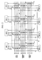
- FIG. 4 shows a connection state of address buses 17 A to 17 D, command buses 16 A to 16 D, and data buses 15 A to 15 D between the four banks 1 , 2 , 3 , and 4 and the four input/output ports A, B, C, and D in the normal operation mode in the route switching circuit 11 of FIG. 2 .
- a contact point shown with a filled circle in boxes that denote crossbar switches 51 to 53 , 61 to 63 , 71 to 73 , and 81 to 83 is in a connected state.
- the port A is connected to the bank 1 via the crossbar switches 51 to 53 .
- the port B is connected to the bank 2 via the crossbar switches 61 to 63 .
- the port C is connected to the bank 3 via the crossbar switches 71 to 73 .
- the port D is connected to the bank 4 via the crossbar switches 81 to 83 .
- the data input/output signal buses of the banks 1 , 2 , 3 , and 4 are essentially 8 bit wide.
- the data input/output bit widths of the ports A, B, C, and D are 8 bit wide.
- FIG. 5 is for explaining an example of DQ integration mode in the route switching circuit 11 of FIG. 2 .
- FIG. 5 shows a connection state of the address buses 17 A to 17 D, the command buses 16 A to 16 D, and the data buses 15 A to 15 D between the four banks 1 , 2 , 3 , and 4 and the four input/output ports A, B, C, and D in the case where a system made of the port A and the bank 1 uses the DQ pins of the port A and the port B.
- the data input/output signal bus of the bank 1 is essentially 16 bit wide.
- This 16-bit wide input/output data signal line is divided into 8-bit widths, each connected to the data bus 15 A and the data bus 15 B by the crossbar switch 51 on the upper left portion that has received a DQ integration signal.
- the 16-bit wide data input/output signal of the bank 1 is divided and connected to the 8-bit wide DQ pin of the port A and the 8-bit wide DQ pin of the port B.
- the DQ integration signal DQ that is input to the ports controls the ports whose DQ pins are integrated (port B, in this example) so that the data input/output timing of the port B is synchronized with the data input/output timing of the ports into which the DQ pins are integrated (port A, in this example).
- a system made of the bank 3 and the port C, and a system made of the bank 4 and the port D are each capable of having access independently of this.
- FIG. 6 is for explaining an example of DQ integration mode in the route switching circuit 11 of FIG. 2 .
- FIG. 6 shows a connection state of the address buses 17 A to 17 D, the command buses 16 A to 16 D, and the data buses 15 A to 15 D between the four banks 1 , 2 , 3 , and 4 and the four input/output ports A, B, C, and D in the case where a system made of the port A and the bank 1 uses the DQ pins of the port A to port D.
- the data input/output signal of the bank 1 is essentially 32 bit wide.
- This 32-bit wide input/output data signal line is divided into 8-bit widths, each connected to the data bus 15 A to the data bus 15 D by the crossbar switch 51 on the upper left portion that has received a DQ integration signal.
- the 32-bit wide data input/output signal of the bank 1 is divided and connected to the 8-bit wide DQ pin of the port A, the 8-bit wide DQ pin of the port B, the 8-bit wide DQ pin of the port C, and the 8-bit wide DQ pin of the port D.
- the DQ integration signal DQ that is input to the ports controls the ports whose DQ pins are integrated (ports B to D, in this example) so that the data input/output timing of the ports B to D is synchronized with the data input/output timing of the ports into which the DQ pins are integrated (port A, in this example).
- FIG. 7 is for explaining an example of DQ integration mode in the route switching circuit 11 of FIG. 2 .
- FIG. 7 shows a connection state of the address buses 17 A to 17 D, the command buses 16 A to 16 D, and the data buses 15 A to 15 D between the four banks 1 , 2 , 3 , and 4 and the four input/output ports A, B, C, and D in the case where a system made of the port A and the bank 1 uses the DQ pins of the port A and the port B and where a system made of the port C and the bank 3 uses the DQ pins of the port C and the port D.
- the data input/output signal bus of the bank 1 is essentially 16 bit wide.
- the data input/output signal of the bank 3 is also essentially 16 bit wide.
- These 16-bit wide input/output data signal lines are divided into 8-bit widths by the crossbar switch 51 in the leftmost and the crossbar switch 71 in the second from the right on the data buses 15 A to 15 D that have received a DQ integration signal.
- the bank 1 is connected to the data buses 15 A and 15 B
- the bank 3 is connected to the data buses 15 C and 15 D.
- the 16-bit wide data input/output signal of the bank 1 is divided and connected to the 8-bit wide DQ pin of the port A and the 8-bit wide DQ pin of the port B.
- the 16-bit wide data input/output signal of the bank 3 is divided and connected to the 8-bit wide DQ pin of the port C and the 8-bit wide DQ pin of the port D.
- the DQ integration signal DQ that is input to the ports controls the data input/output timing of the ports whose DQ pins are integrated (ports B and D, in this example) so that the data input/output timing of the ports B and D is synchronized with the data input/output timing of the ports into which the DQ pins are integrated (port A and C, in this example).
- FIG. 8 shows an exemplary configuration of a computer system including: a multi-core processor 100 with four CPU cores; and a multi-port memory 110 according to an embodiment of the present invention.
- the multi-core processor 100 includes four CPU cores: core 101 , core 102 , core 103 , and core 104 .
- the multi-core processor 100 includes: an I/O 105 that functions as an interface with an external circuit; an external storage apparatus control block 106 ; and an on-chip memory 107 .
- the multi-port memory 110 functions as an external storage apparatus for the multi-core processor 100 .
- the external storage apparatus control block 106 of the processor chip controls the multi-port memory 110 .
- the external storage apparatus control block 106 it is possible for the external storage apparatus control block 106 to allocate four CPU cores 101 , 102 , 103 , and 104 of the multi-core processor to four ports of the multi-port memory 110 .
- a plurality of banks are allocated to a plurality of CPU cores via one ore more input/output ports.
- data transfer load of an input/output port exceeds the limit of its data transfer capability during the period of time when a data transfer of another input/output port is not performed, it is possible to integrate data signal lines of the input/output ports where no transfer is performed into the data signal line of the input/output port where the data transfer capability has exceeded its limit, to thereby dynamically improve the data transfer capability. Therefore, in a system that uses a multi-core processor, a data transfer time with memory is unlikely to be a bottleneck, to thereby make it possible to improve the performance of the system.
- a computer system described above may be adapted to a computer system which uses single-core processor.
Abstract
Description
Claims (10)
Applications Claiming Priority (2)
| Application Number | Priority Date | Filing Date | Title |
|---|---|---|---|
| JP2008071461A JP5599969B2 (en) | 2008-03-19 | 2008-03-19 | Multi-port memory and computer system including the multi-port memory |
| JPP2008-071461 | 2008-03-19 |
Publications (2)
| Publication Number | Publication Date |
|---|---|
| US20090240866A1 US20090240866A1 (en) | 2009-09-24 |
| US8006026B2 true US8006026B2 (en) | 2011-08-23 |
Family
ID=41089993
Family Applications (1)
| Application Number | Title | Priority Date | Filing Date |
|---|---|---|---|
| US12/382,524 Active US8006026B2 (en) | 2008-03-19 | 2009-03-18 | Multi-port memory and computer system provided with the same |
Country Status (2)
| Country | Link |
|---|---|
| US (1) | US8006026B2 (en) |
| JP (1) | JP5599969B2 (en) |
Cited By (3)
| Publication number | Priority date | Publication date | Assignee | Title |
|---|---|---|---|---|
| US20100312939A1 (en) * | 2009-06-08 | 2010-12-09 | Commiss. A L'energie Atom. Et Aux Energ. Alterna. | Interconnection network with dynamic sub-networks |
| US9514069B1 (en) | 2012-05-24 | 2016-12-06 | Schwegman, Lundberg & Woessner, P.A. | Enhanced computer processor and memory management architecture |
| US20190317799A1 (en) * | 2018-04-16 | 2019-10-17 | Stmicroelectronics (Rousset) Sas | Method for managing transactions routing between source equipment and target equipment |
Families Citing this family (6)
| Publication number | Priority date | Publication date | Assignee | Title |
|---|---|---|---|---|
| US8407427B2 (en) | 2008-10-29 | 2013-03-26 | Silicon Image, Inc. | Method and system for improving serial port memory communication latency and reliability |
| US9152585B2 (en) * | 2009-02-12 | 2015-10-06 | Rambus Inc. | Memory interface with reduced read-write turnaround delay |
| US8769213B2 (en) * | 2009-08-24 | 2014-07-01 | Micron Technology, Inc. | Multi-port memory and operation |
| JP5864957B2 (en) | 2011-08-31 | 2016-02-17 | ルネサスエレクトロニクス株式会社 | Semiconductor device |
| US10387299B2 (en) * | 2016-07-20 | 2019-08-20 | Micron Technology, Inc. | Apparatuses and methods for transferring data |
| WO2020197964A1 (en) * | 2019-03-26 | 2020-10-01 | Axis Semiconductor, Inc. | Computing device with circuit switched memory access |
Citations (18)
| Publication number | Priority date | Publication date | Assignee | Title |
|---|---|---|---|---|
| JPH05342856A (en) | 1992-06-04 | 1993-12-24 | Matsushita Electron Corp | Random access semiconductor memory device |
| JPH08221319A (en) | 1995-02-13 | 1996-08-30 | Hitachi Ltd | Semiconductor memory device |
| US5657289A (en) | 1995-08-30 | 1997-08-12 | Micron Technology, Inc. | Expandable data width SAM for a multiport RAM |
| US5799209A (en) | 1995-12-29 | 1998-08-25 | Chatter; Mukesh | Multi-port internally cached DRAM system utilizing independent serial interfaces and buffers arbitratively connected under a dynamic configuration |
| JP2000215659A (en) | 1999-01-27 | 2000-08-04 | Fujitsu Ltd | Semiconductor memory and information processor |
| JP2000243079A (en) | 1999-02-19 | 2000-09-08 | Nec Corp | Semiconductor integrated circuit device |
| US6212597B1 (en) | 1997-07-28 | 2001-04-03 | Neonet Lllc | Apparatus for and method of architecturally enhancing the performance of a multi-port internally cached (AMPIC) DRAM array and like |
| US20010007122A1 (en) * | 1998-03-05 | 2001-07-05 | Robert Cohen | Multi-port memory device with multiple modes of operation and improved expansion characteristics |
| US20020078311A1 (en) | 2000-12-20 | 2002-06-20 | Fujitsu Limited | Multi-port memory based on DRAM core |
| JP2002197858A (en) | 2000-12-27 | 2002-07-12 | Fujitsu Ltd | Semiconductor memory |
| US20030135699A1 (en) | 2000-12-20 | 2003-07-17 | Yasurou Matsuzaki | Multi-port memory based on DRAM core |
| JP2003263363A (en) | 2002-03-08 | 2003-09-19 | Ricoh Co Ltd | Memory control circuit |
| JP2003272378A (en) | 2002-03-14 | 2003-09-26 | Fujitsu Ltd | Semiconductor memory device |
| US6850954B2 (en) | 2001-01-18 | 2005-02-01 | Noriaki Kawamae | Information retrieval support method and information retrieval support system |
| US20050268023A1 (en) | 2004-06-01 | 2005-12-01 | Briggs Randall D | Multi-port random access memory |
| US20070147162A1 (en) | 2005-12-22 | 2007-06-28 | Samsung Electronics Co., Ltd. | Multi-port semiconductor memory device having variable access paths and method therefor |
| US20080077747A1 (en) * | 2006-09-21 | 2008-03-27 | Hynix Semiconductor Inc. | Multi-port memory device |
| US20090254698A1 (en) * | 2008-02-27 | 2009-10-08 | Samsung Electronics Co., Ltd. | Multi port memory device with shared memory area using latch type memory cells and driving method |
Family Cites Families (2)
| Publication number | Priority date | Publication date | Assignee | Title |
|---|---|---|---|---|
| JPH07113916B2 (en) * | 1986-12-27 | 1995-12-06 | 株式会社ピーエフユー | Complex computer system |
| JP2006260127A (en) * | 2005-03-17 | 2006-09-28 | Hiroshima Univ | Interconnection network and multiport memory using the same |
-
2008
- 2008-03-19 JP JP2008071461A patent/JP5599969B2/en not_active Expired - Fee Related
-
2009
- 2009-03-18 US US12/382,524 patent/US8006026B2/en active Active
Patent Citations (26)
| Publication number | Priority date | Publication date | Assignee | Title |
|---|---|---|---|---|
| JPH05342856A (en) | 1992-06-04 | 1993-12-24 | Matsushita Electron Corp | Random access semiconductor memory device |
| JPH08221319A (en) | 1995-02-13 | 1996-08-30 | Hitachi Ltd | Semiconductor memory device |
| US5657289A (en) | 1995-08-30 | 1997-08-12 | Micron Technology, Inc. | Expandable data width SAM for a multiport RAM |
| US5717647A (en) | 1995-08-30 | 1998-02-10 | Micron Technology, Inc. | Expandable data width sam for a multiport ram |
| JPH10511208A (en) | 1995-08-30 | 1998-10-27 | マイクロン・テクノロジー・インコーポレーテッド | SAM with expandable data width for multiport RAM |
| US6108725A (en) | 1995-12-29 | 2000-08-22 | Chatter; Mukesh | Multi-port internally cached DRAM system utilizing independent serial interfaces and buffers arbitratively connected under a dynamic configuration to allow access to a common internal bus |
| US5799209A (en) | 1995-12-29 | 1998-08-25 | Chatter; Mukesh | Multi-port internally cached DRAM system utilizing independent serial interfaces and buffers arbitratively connected under a dynamic configuration |
| JP2000501524A (en) | 1995-12-29 | 2000-02-08 | チャッター,マケッシュ | High performance universal multiport internal cache dynamic random access memory system, structure and method |
| JP2001511559A (en) | 1997-07-28 | 2001-08-14 | ネグザビット・ネットワークス,リミテッド・ライアビリティー・カンパニー | Multi-port internal cache DRAM |
| US6212597B1 (en) | 1997-07-28 | 2001-04-03 | Neonet Lllc | Apparatus for and method of architecturally enhancing the performance of a multi-port internally cached (AMPIC) DRAM array and like |
| US20010007122A1 (en) * | 1998-03-05 | 2001-07-05 | Robert Cohen | Multi-port memory device with multiple modes of operation and improved expansion characteristics |
| JP2000215659A (en) | 1999-01-27 | 2000-08-04 | Fujitsu Ltd | Semiconductor memory and information processor |
| JP2000243079A (en) | 1999-02-19 | 2000-09-08 | Nec Corp | Semiconductor integrated circuit device |
| US20020078311A1 (en) | 2000-12-20 | 2002-06-20 | Fujitsu Limited | Multi-port memory based on DRAM core |
| US20030135699A1 (en) | 2000-12-20 | 2003-07-17 | Yasurou Matsuzaki | Multi-port memory based on DRAM core |
| JP2002197858A (en) | 2000-12-27 | 2002-07-12 | Fujitsu Ltd | Semiconductor memory |
| US6850954B2 (en) | 2001-01-18 | 2005-02-01 | Noriaki Kawamae | Information retrieval support method and information retrieval support system |
| JP2003263363A (en) | 2002-03-08 | 2003-09-19 | Ricoh Co Ltd | Memory control circuit |
| JP2003272378A (en) | 2002-03-14 | 2003-09-26 | Fujitsu Ltd | Semiconductor memory device |
| US20050268023A1 (en) | 2004-06-01 | 2005-12-01 | Briggs Randall D | Multi-port random access memory |
| JP2005346715A (en) | 2004-06-01 | 2005-12-15 | Agilent Technol Inc | Multiport random access memory |
| US20070147162A1 (en) | 2005-12-22 | 2007-06-28 | Samsung Electronics Co., Ltd. | Multi-port semiconductor memory device having variable access paths and method therefor |
| JP2007172811A (en) | 2005-12-22 | 2007-07-05 | Samsung Electronics Co Ltd | Multi-port semiconductor memory device having variable access paths, and method therefor |
| US7505353B2 (en) | 2005-12-22 | 2009-03-17 | Samsung Electronics Co., Ltd. | Multi-port semiconductor memory device having variable access paths and method |
| US20080077747A1 (en) * | 2006-09-21 | 2008-03-27 | Hynix Semiconductor Inc. | Multi-port memory device |
| US20090254698A1 (en) * | 2008-02-27 | 2009-10-08 | Samsung Electronics Co., Ltd. | Multi port memory device with shared memory area using latch type memory cells and driving method |
Cited By (5)
| Publication number | Priority date | Publication date | Assignee | Title |
|---|---|---|---|---|
| US20100312939A1 (en) * | 2009-06-08 | 2010-12-09 | Commiss. A L'energie Atom. Et Aux Energ. Alterna. | Interconnection network with dynamic sub-networks |
| US8397009B2 (en) * | 2009-06-08 | 2013-03-12 | Commissariat A L'energie Atomique Et Aux Energies Alternatives | Interconnection network with dynamic sub-networks |
| US9514069B1 (en) | 2012-05-24 | 2016-12-06 | Schwegman, Lundberg & Woessner, P.A. | Enhanced computer processor and memory management architecture |
| US20190317799A1 (en) * | 2018-04-16 | 2019-10-17 | Stmicroelectronics (Rousset) Sas | Method for managing transactions routing between source equipment and target equipment |
| US10740141B2 (en) * | 2018-04-16 | 2020-08-11 | Stmicroelectronics (Rousset) Sas | Method for managing transactions routing between source equipment and target equipment |
Also Published As
| Publication number | Publication date |
|---|---|
| JP2009230776A (en) | 2009-10-08 |
| US20090240866A1 (en) | 2009-09-24 |
| JP5599969B2 (en) | 2014-10-01 |
Similar Documents
| Publication | Publication Date | Title |
|---|---|---|
| US8006026B2 (en) | Multi-port memory and computer system provided with the same | |
| US11687454B2 (en) | Memory circuit and cache circuit configuration | |
| US7222224B2 (en) | System and method for improving performance in computer memory systems supporting multiple memory access latencies | |
| US8209497B2 (en) | Multi-port memory and system using the same | |
| US9047942B2 (en) | Non-transitory computer-readable media describing a hybrid volatile and non-volatile memory device with an overlapping region of addressable range of storage cells | |
| US7136958B2 (en) | Multiple processor system and method including multiple memory hub modules | |
| US7840762B2 (en) | Multi-path accessible semiconductor memory device having mailbox areas and mailbox access control method thereof | |
| US7451263B2 (en) | Shared interface for components in an embedded system | |
| US7596666B2 (en) | Multi-path accessible semiconductor memory device having port state signaling function | |
| US20080256305A1 (en) | Multipath accessible semiconductor memory device | |
| JP2009259392A (en) | Memory architecture | |
| US20090089487A1 (en) | Multiport semiconductor memory device having protocol-defined area and method of accessing the same | |
| KR20000011417A (en) | Semiconductor integrated circuit and data processing system | |
| US7398362B1 (en) | Programmable interleaving in multiple-bank memories | |
| US11474950B2 (en) | Memory controller including plurality of address mapping tables, system on chip, and electronic device | |
| US9696941B1 (en) | Memory system including memory buffer | |
| JP2002109884A (en) | Memory device | |
| RU2481652C1 (en) | Integrated circuit with multi-port super memory cell and circuit of data transfer route switching | |
| US7996601B2 (en) | Apparatus and method of partially accessing dynamic random access memory | |
| US20210349839A1 (en) | Multi-ported nonvolatile memory device with bank allocation and related systems and methods | |
| US20130031347A1 (en) | Arrangement and method | |
| US7986582B2 (en) | Method of operating a memory apparatus, memory device and memory apparatus | |
| US8244929B2 (en) | Data processing apparatus | |
| US7586779B2 (en) | Controller apparatus for utilizing downgrade memory and method for operating the same | |
| KR20170128783A (en) | Memory system and operation method of the same |
Legal Events
| Date | Code | Title | Description |
|---|---|---|---|
| AS | Assignment |
Owner name: ELPIDA MEMORY, INC., JAPAN Free format text: ASSIGNMENT OF ASSIGNORS INTEREST;ASSIGNOR:KAJIGAYA, KAZUHIKO;REEL/FRAME:022465/0808 Effective date: 20090317 |
|
| STCF | Information on status: patent grant |
Free format text: PATENTED CASE |
|
| FEPP | Fee payment procedure |
Free format text: PAYOR NUMBER ASSIGNED (ORIGINAL EVENT CODE: ASPN); ENTITY STATUS OF PATENT OWNER: LARGE ENTITY |
|
| AS | Assignment |
Owner name: ELPIDA MEMORY INC., JAPAN Free format text: SECURITY AGREEMENT;ASSIGNOR:PS4 LUXCO S.A.R.L.;REEL/FRAME:032414/0261 Effective date: 20130726 |
|
| AS | Assignment |
Owner name: PS4 LUXCO S.A.R.L., LUXEMBOURG Free format text: ASSIGNMENT OF ASSIGNORS INTEREST;ASSIGNOR:ELPIDA MEMORY, INC.;REEL/FRAME:032896/0353 Effective date: 20130726 |
|
| FEPP | Fee payment procedure |
Free format text: PAYER NUMBER DE-ASSIGNED (ORIGINAL EVENT CODE: RMPN); ENTITY STATUS OF PATENT OWNER: LARGE ENTITY Free format text: PAYOR NUMBER ASSIGNED (ORIGINAL EVENT CODE: ASPN); ENTITY STATUS OF PATENT OWNER: LARGE ENTITY |
|
| FPAY | Fee payment |
Year of fee payment: 4 |
|
| AS | Assignment |
Owner name: PS5 LUXCO S.A.R.L., LUXEMBOURG Free format text: ASSIGNMENT OF ASSIGNORS INTEREST;ASSIGNOR:PS4 LUXCO S.A.R.L.;REEL/FRAME:039818/0506 Effective date: 20130829 Owner name: LONGITUDE SEMICONDUCTOR S.A.R.L., LUXEMBOURG Free format text: CHANGE OF NAME;ASSIGNOR:PS5 LUXCO S.A.R.L.;REEL/FRAME:039793/0880 Effective date: 20131112 |
|
| AS | Assignment |
Owner name: LONGITUDE LICENSING LIMITED, IRELAND Free format text: ASSIGNMENT OF ASSIGNORS INTEREST;ASSIGNOR:LONGITUDE SEMICONDUCTOR S.A.R.L.;REEL/FRAME:046865/0667 Effective date: 20180731 |
|
| MAFP | Maintenance fee payment |
Free format text: PAYMENT OF MAINTENANCE FEE, 8TH YEAR, LARGE ENTITY (ORIGINAL EVENT CODE: M1552); ENTITY STATUS OF PATENT OWNER: LARGE ENTITY Year of fee payment: 8 |
|
| MAFP | Maintenance fee payment |
Free format text: PAYMENT OF MAINTENANCE FEE, 12TH YEAR, LARGE ENTITY (ORIGINAL EVENT CODE: M1553); ENTITY STATUS OF PATENT OWNER: LARGE ENTITY Year of fee payment: 12 |