US8856423B1 - Dual-purpose nonvolatile memory for code and data storage - Google Patents
Dual-purpose nonvolatile memory for code and data storage Download PDFInfo
- Publication number
- US8856423B1 US8856423B1 US11/789,971 US78997107A US8856423B1 US 8856423 B1 US8856423 B1 US 8856423B1 US 78997107 A US78997107 A US 78997107A US 8856423 B1 US8856423 B1 US 8856423B1
- Authority
- US
- United States
- Prior art keywords
- memory
- interface
- code
- solid
- control module
- Prior art date
- Legal status (The legal status is an assumption and is not a legal conclusion. Google has not performed a legal analysis and makes no representation as to the accuracy of the status listed.)
- Active, expires
Links
Images


Classifications
-
- G—PHYSICS
- G06—COMPUTING; CALCULATING OR COUNTING
- G06F—ELECTRIC DIGITAL DATA PROCESSING
- G06F12/00—Accessing, addressing or allocating within memory systems or architectures
- G06F12/02—Addressing or allocation; Relocation
- G06F12/0223—User address space allocation, e.g. contiguous or non contiguous base addressing
- G06F12/023—Free address space management
- G06F12/0238—Memory management in non-volatile memory, e.g. resistive RAM or ferroelectric memory
- G06F12/0246—Memory management in non-volatile memory, e.g. resistive RAM or ferroelectric memory in block erasable memory, e.g. flash memory
Definitions
- the present disclosure relates to data processing systems, and more particularly to storing program code and data in a dual-purpose nonvolatile storage system.
- Data processing systems include processors that execute program code and process data.
- the program code such as an operating system (OS) includes a set of commands or instructions that a processor executes to process data.
- OS operating system
- a data processing system 10 includes a processor 12 , a disk drive 14 , a host adapter 16 , and a system memory 18 .
- the processor 12 , the host adapter 16 , and the system memory 18 communicate via a system bus 20 .
- the disk drive 14 stores data on magnetic surfaces.
- the disk drive 14 communicates with the host adapter 16 via a standard I/O interface 24 such as ATA, SATA, USB, etc.
- the host adapter 16 reads the code and data from the disk drive 14 into the system memory 18 .
- the processor 12 reads the code and data from the system memory 18 , executes the code, and processes the data in the system memory 18 .
- the host adapter 16 may read the processed data from the system memory 18 and store the processed data in the disk drive 14 .
- the disk drive 14 stores the code and data in a nonvolatile manner.
- the disk drive 14 can provide the code and data to the processor 12 every time power is turned on.
- the disk drive 14 provides code and data to the processor 12 at a rate that is slower than the rate at which the processor 12 can execute the code and process the data.
- the system memory 18 is generally volatile. That is, contents of the system memory 18 may be lost when power is turned off. But the system memory 18 can provide the code and data to the processor 12 faster than the disk drive 14 .
- the processor 12 may execute the code and process the data from the system memory 18 while the host adapter 16 loads additional portions of the code and/or data into the system memory 18 .
- the processor 12 can execute the code and process the data from the system memory 18 faster than the rate at which the host adapter 16 can load additional code and data into the system memory 18 from the disk drive 14 .
- the system memory 18 is generally volatile, the host adapter 16 needs to load portions of the code and data into the system memory 18 every time power is turned on. Thus, the processor 12 may wait until portions of the code and data are loaded into the system memory 18 .
- a control module for controlling a solid-state disk comprises a first interface, a cache memory, and a second interface.
- the first interface interfaces a nonvolatile semiconductor memory (NVM) of the SSD to a processor that is located externally to the SSD.
- the cache memory selectively caches at least one of code and data from the NVM.
- the second interface interfaces the cache memory to the processor and outputs portions of at least one of code and data from the cache memory to the processor.
- control module reads at least one of code and data from the NVM into the cache memory when the processor communicates N requests for at least one of code and data to the SSD, where N is an integer greater than or equal to 1.
- the NVM comprises flash memory.
- the cache memory comprises one of volatile and nonvolatile memory.
- the cache memory comprises one of static random access memory (SRAM), flash memory, and magnetic RAM.
- SRAM static random access memory
- flash memory flash memory
- magnetic RAM magnetic random access memory
- the second interface comprises a parallel interface.
- first and second interfaces are implemented by a combined interface.
- an integrated circuit comprises the control module.
- a solid-state disk comprises the control module and further comprises the NVM and volatile memory, wherein the control module reads at least one of code and data from the NVM into the volatile memory, and wherein the cache memory caches at least one of code and data from the volatile memory.
- a handheld device comprises the SSD and further comprises a bus, a host adapter that communicates with the bus, and the processor that communicates with the first interface via the host adapter.
- a method comprises providing a solid-state disk (SSD) having a nonvolatile semiconductor memory (NVM) and a control module and controlling the SSD using the control module having a cache memory and first and second interfaces.
- the method further comprises selectively caching at least one of code and data from the NVM to the cache memory.
- the method further comprises interfacing the NVM to a processor located externally to the SSD via the first interface and interfacing the cache memory to the processor via the second interface.
- the method further comprises outputting portions of at least one of code and data from the cache memory to the processor via the second interface.
- the method further comprises reading at least one of code and data from the NVM into the cache memory when the processor communicates N requests for at least one of code and data to the SSD, where N is an integer greater than or equal to 1.
- the NVM comprises flash memory.
- the cache memory comprises one of volatile and nonvolatile memory.
- the cache memory comprises one of static random access memory (SRAM), flash memory, and magnetic RAM.
- SRAM static random access memory
- flash memory flash memory
- magnetic RAM magnetic random access memory
- the method further comprises implementing the second interface using a parallel interface.
- the method further comprises combining the first and second interfaces.
- the method further comprises arranging the control module in an integrated circuit (IC).
- IC integrated circuit
- the method further comprises providing a volatile memory in the SSD, reading at least one of code and data from the NVM into the volatile memory, and caching at least one of code and data from the volatile memory.
- the method further comprises providing the SSD, the processor, a host adapter, and a bus in a handheld device.
- the method further comprises transmitting at least one of code and data from the NVM to the processor via the first interface and the host adapter.
- the method further comprises transmitting the portions of at least one of code and data from the cache memory to the processor via the second interface.
- a control module for controlling a solid-state disk comprises first interface means for interfacing a nonvolatile semiconductor memory (NVM) of the SSD to a processor that is located externally to the SSD.
- the control module further comprises cache memory means for selectively caching at least one of code and data from the NVM.
- the control module further comprises second interface means for interfacing the cache memory means to the processor and outputting portions of at least one of code and data from the cache memory means to the processor.
- control module reads at least one of code and data from the NVM into the cache memory means when the processor communicates N requests for at least one of code and data to the SSD, where N is an integer greater than or equal to 1.
- the NVM comprises flash memory.
- the cache memory means comprises one of volatile and nonvolatile memory means for storing data.
- the cache memory means comprises one of static random access memory (SRAM) means for storing data, flash memory means for storing data, and magnetic RAM means for storing data.
- SRAM static random access memory
- the second interface means comprises parallel interface means for interfacing the cache memory means to the processor.
- first and second interface means are implemented by combined interface means for interfacing the control module to the processor.
- an integrated circuit comprises the control module.
- a solid-state disk comprises the control module and further comprises the NVM and volatile memory, wherein the control module reads at least one of code and data from the NVM into the volatile memory, and wherein the cache memory means caches at least one of code and data from the volatile memory.
- a handheld device comprises the SSD and further comprises a bus, a host adapter that communicates with the bus, and the processor that communicates with the first interface means via the host adapter.
- FIG. 1 is a functional block diagram of an exemplary computing system according to the prior art
- FIG. 2A is a functional block diagram of an exemplary computing system
- FIG. 2B is a functional block diagram of an exemplary solid-state disk
- FIG. 3A is a functional block diagram of an exemplary computing system according to the present disclosure.
- FIG. 3B is a functional block diagram of an exemplary solid-state disk according to the present disclosure.
- FIG. 4A is a functional block diagram of an exemplary control module used in a solid-state disk according to the present disclosure
- FIG. 4B is a functional block diagram of an exemplary solid-state disk according to the present disclosure.
- FIG. 5A shows an exemplary connector of a solid-state disk according to the present disclosure
- FIG. 5B shows exemplary connections of a connector of a solid-state disk according to the present disclosure
- FIG. 5C shows exemplary connections of a connector of a solid-state disk according to the present disclosure
- FIGS. 6A and 6B are flowcharts of exemplary methods for implementing memory in a solid-state disk, where the memory may be interfaced directly to a remote processor according to the present disclosure
- FIG. 7A is a functional block diagram of a cellular phone.
- FIG. 7B is a functional block diagram of a media player.
- module, circuit and/or device refers to an Application Specific Integrated Circuit (ASIC), an electronic circuit, a processor (shared, dedicated, or group) and memory that execute one or more software or firmware programs, a combinational logic circuit, and/or other suitable components that provide the described functionality.
- ASIC Application Specific Integrated Circuit
- processor shared, dedicated, or group
- memory that execute one or more software or firmware programs, a combinational logic circuit, and/or other suitable components that provide the described functionality.
- phrase at least one of A, B, and C should be construed to mean a logical (A or B or C), using a non-exclusive logical or. It should be understood that steps within a method may be executed in different order without altering the principles of the present disclosure.
- Modern handheld electronic devices such as personal digital assistants (PDAs) and cellular phones may include data processing systems (systems) that can perform complex functions.
- PDAs personal digital assistants
- cellular phones that are equipped with a camera may include systems that can take pictures, manipulate the pictures, and communicate the pictures via the Internet.
- PDAs may include systems that can download, process, and upload video files via the Internet. Performance of these systems can be enhanced by increasing the rate at which code and data is provided to processors in these devices.
- Various storage schemes may be used to improve the rate of providing code and data to a processor.
- a solid-state disk which has a faster access time than a disk drive that uses rotating magnetic medium, may be used instead of the disk drive to store the code and data.
- flash memory which is nonvolatile and rewritable, may be used to store portions of the code.
- the flash memory may be interfaced directly to the processor.
- the processor may execute the portions of the code stored in the flash memory without waiting for the disk drive to provide that information.
- a system 11 includes the processor 12 , a solid-state disk (SSD) 22 , the host adapter 16 , a flash memory 26 , and the system memory 18 .
- the processor 12 , the host adapter 16 , and the system memory 18 communicate via the system bus 20 as shown in FIG. 2A .
- the flash memory 26 may be interfaced directly to the processor 12 via a flash memory interface 27 .
- the SSD 22 stores code and data.
- the SSD 22 communicates with the host adapter 16 via a standard I/O interface 24 such as ATA, SATA, USB, etc.
- the host adapter 16 reads the code and the data from the SSD 22 into the system memory 18 .
- the processor 12 reads the code and data from the system memory 18 , executes the code, and processes the data in the system memory 18 .
- the host adapter 16 may read the processed data from the system memory 18 and store the processed data in the SSD 22 .
- the SSD 22 may comprise a nonvolatile semiconductor memory (NVM) 30 , a control module 32 , and a volatile memory 34 such as dynamic random-access memory (DRAM) as shown in FIG. 2B .
- the NVM 30 stores the code and the data.
- the NVM 30 may include flash memory such as NAND flash.
- NAND flash is nonvolatile and rewritable sequential-access memory that functions like a disk drive. The access time of NAND flash, however, is faster than the access time of the disk drive. Thus, the SSD 22 can provide the code and data to the processor 12 faster than the disk drive.
- the control module 32 reads the code from the NVM 30 , reads/writes data from/to the NVM 30 , erases blocks of the NVM 30 , corrects errors, etc.
- the control module 32 may use volatile memory 34 such as dynamic random-access memory (DRAM) for temporarily storing information related to the control and operation of the SSD 22 .
- the control module 32 provides the I/O interface 24 that communicates with a connector 25 .
- the SSD 22 connects to the host adapter 16 via the connector 25 .
- the processor 12 may read the portions of the code from the SSD 22 into the flash memory 26 . Subsequently, the processor 12 may read the portions of the code directly from the flash memory 26 and readily execute the portions of the code. Thus, the processor 12 may not wait for the host adapter 16 to load the portions of the code from the SSD 22 into the system memory 18 and subsequently retrieve the portions of the code from the system memory 18 .
- the flash memory 26 may include NOR flash, which is an execute-in-place (XIP) memory like read-only memory (ROM). Since NOR flash can be accessed randomly, NOR flash may provide the code to the processor 12 faster than the SSD 22 and the disk drive. In addition to storing the portions of the code, the flash memory 26 may be used to store portions of data that the processor 12 may access and/or process repeatedly.
- NOR flash is an execute-in-place (XIP) memory like read-only memory (ROM). Since NOR flash can be accessed randomly, NOR flash may provide the code to the processor 12 faster than the SSD 22 and the disk drive. In addition to storing the portions of the code, the flash memory 26 may be used to store portions of data that the processor 12 may access and/or process repeatedly.
- the devices may use SSDs to store code and data. Additionally, the devices may include flash memory that is located outside the SSD and that is interfaced directly to a processor in the devices.
- the flash memory may be used to store portions of code that the processor may execute.
- the processor can read the portions of the code directly from the flash memory and readily execute the portions of the code. Additionally, if the processor executes the portions of the code repeatedly or frequently, the processor need not wait for the code to be read again when the code is stored in the flash memory.
- Including flash memory in the devices in addition to the SSD may increase hardware costs of the devices.
- an internal memory such as cache memory
- flash memory or magnetic RAM may be included in the SSD to store portions of the code according to the present disclosure.
- the internal memory in the SSD may be interfaced directly to the processor via a memory interface that is distinct from an I/O interface with which the SSD communicates with a host adapter.
- the processor may directly access the internal memory, read the portions of the code from the internal memory, and readily execute the code, thereby eliminating the need for separate memory that is located externally to the SSD and that is coupled to the processor specifically for storing portions of the code.
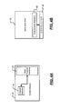
- a data processing system 40 may comprise the processor 12 , a solid-state disk (disk) 50 , the host adapter 16 , and the system memory 18 .
- the processor 12 , the host adapter 16 , and the system memory 18 communicate via the system bus 20 .
- the disk 50 stores the code and data.
- the disk 50 communicates with the host adapter 16 via a standard I/O interface 58 such as ATA, SATA, USB, etc.
- the host adapter 16 reads the code and data from the disk 50 into the system memory 18 .
- the processor 12 reads the code from the system memory 18 , executes the code, and processes the data in the system memory 18 .
- the host adapter 16 may read the processed data from the system memory 18 and store the processed data in the disk 50 .
- the disk 50 may comprise the NVM 30 , a control module 52 , and the volatile memory 34 such as DRAM.
- the NVM 30 stores the code and the data.
- the NVM 30 may include flash memory such as NAND flash.
- NAND flash is nonvolatile and rewritable sequential-access memory that functions like a disk drive. The access time of NAND flash is faster than the access time of the disk drive. Thus, the disk 50 can provide code and data to the processor 12 faster than the disk drive.
- the control module 52 reads the code from the NVM 30 , reads/writes data from/to the NVM 30 , erases blocks of the NVM 30 , corrects errors, etc.
- the control module 52 may use the volatile memory 34 such as DRAM for temporarily storing information related to the control and operation of the disk 50 .
- control module 52 comprises an internal memory 54 (also called cache memory).
- the internal memory 54 is interfaced directly to the processor 12 via a memory interface 56 .
- the memory interface 56 provides a random-access interface with which the processor 12 directly accesses the internal memory 54 .
- the control module 52 may read the portions of the code from the NVM 30 into the internal memory 54 .
- the control module 52 may read the portions of the code from the NVM 30 into the internal memory 54 .
- the control module 52 may read the portions of the code from the NVM 30 into the volatile memory 34 and subsequently load the portions of the code from the volatile memory 34 into the internal memory 54 .
- the processor 12 may directly access the internal memory 54 via the memory interface 56 , read the portions of the code stored into the internal memory 54 , and execute the portions of the code. Thus, the processor 12 may not wait for the host adapter 16 to read the portions of the code from the disk 50 into the system memory 18 and subsequently retrieve the portions of the code from the system memory 18 .
- internal memory 54 may be used to store portions of data that the processor 12 may access and/or process repeatedly.
- the internal memory 54 may be volatile or nonvolatile and may include any low-latency memory having a fast access time.
- the internal memory 54 may include volatile memory such as static random access memory (SRAM) or magnetic RAM.
- the internal memory 54 may include nonvolatile memory such as NOR flash.
- the memory interface 56 may be compatible with the type of memory used to implement the internal memory 54 .
- the memory interface 56 may include a NOR flash interface if NOR flash is used to implement the internal memory 54 .
- the memory interface 56 provides a parallel interface that provides the processor 12 random access to the internal memory 54 .
- the parallel interface transmits and receives all bits of information in a byte or a codeword simultaneously.
- the control module 52 may provide at least one of the I/O interface 58 and the memory interface 56 .
- the I/O interface 58 and the memory interface 56 may communicate with a connector 60 .
- the disk 50 may communicate with the host adapter 16 and the processor 12 via the connector 60 .
- control module 52 may implement the I/O interface 58 and the memory interface 56 by a dual-purpose purpose interface 62 .
- the dual-purpose interface 62 may communicate with the connector 60 .
- the disk 50 may communicate with the host adapter 16 and the processor 12 via the dual-purpose interface 62 .
- the connector 60 may comprise a first connector 60 - 1 that communicates with the memory interface 56 and a second connector 60 - 2 that communicates with the I/O interface 58 as shown in FIG. 5A .
- the connector 60 may comprise an edge connector that includes edge connections 66 - 1 , 66 - 2 , 66 - 3 , etc. (collectively, edge connections 66 ) as shown in FIG. 5B .
- the connector 60 may include pin connections 68 - 1 , 68 - 2 , 68 - 3 , etc. (collectively, pin connections 68 ) as shown in FIG. 5C , wherein the pin connections 68 may be male, female, or a combination of both.
- the connector 60 may include both edge connections 66 and pin connections 68 .
- the first connector 60 - 1 may include pin connections 68
- the second connector 60 - 2 may include edge connections 66 , or vice versa. Additional implementations including multiplexing edge connections 66 and/or pin connections 68 to provide non-concurrent memory access across both the memory interface 56 and the I/O interface 58 are contemplated.
- the disk 50 may be installed in a handheld device in a removable manner.
- the control module 52 may be installed in the disk 50 in a removable manner.
- At least one of the control module 52 , the volatile memory 34 , and the NVM 30 may be implemented by a single module or a single integrated circuit (IC).
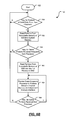
- the control module 52 determines in step 104 if the processor 12 requests portions of code (or data). If false, the control module 52 repeats step 104 . If true, the control module 52 reads the portions from the NVM 30 into the internal memory 54 in step 110 . The control module 52 provides the processor 12 a direct access to the portions stored in the internal memory 54 via the memory interface 56 in step 112 . The control module 52 determines in step 114 if the processor 12 requests the same portions again. If true, the control module 52 repeats step 112 . If false, the control module 52 repeats steps 104 through 114 .
- a method 150 for implementing the internal memory 54 in the solid-state disk (disk) 50 , where the internal memory 54 can be interfaced directly to the remote processor 12 is shown.
- the method 150 begins at step 152 .
- the control module 52 that comprises the internal memory 54 determines in step 154 if the processor 12 requests portions of code and/or data. If false, the control module 52 repeats step 154 . If true, the control module 52 reads the portions from the NVM 30 of the disk 50 into system memory 18 in step 156 , where the system memory 18 , the processor 12 , and the disk 50 communicate via the system bus 20 .
- the control module 52 determines in step 158 if the processor 12 requests the same portions frequently. If false, however, the control module 52 repeats steps 154 through 158 . If true, the control module 52 reads the portions from the NVM 30 into the internal memory 54 in step 160 . The control module 52 provides the processor 12 a direct access to the portions stored in the internal memory 54 via the memory interface 56 in step 162 . The control module 52 determines in step 164 if the processor 12 requests the same portions again. If true, the control module 52 repeats step 162 . If false, the control module 52 repeats steps 154 through 164 .
- the teachings of the present disclosure can be implemented in a mass data storage 464 of a cellular phone 450 that may include a cellular antenna 451 .
- the cellular phone 450 includes a microphone 456 , an audio output 458 such as a speaker and/or audio output jack, a display 460 , and/or an input device 462 such as a keypad, a pointing device, and/or other input device.
- a signal processing and/or control circuit 452 and/or other circuits (not shown) in the cellular phone 450 may process data, perform coding and/or encryption, perform calculations, format data, and/or perform other cellular phone functions.
- the cellular phone 450 may communicate with the mass data storage 464 that stores data in a nonvolatile manner.
- the mass data storage 464 may include a magnetic storage device such as a hard disk drive (HDD), a solid-state disk, and/or an optical storage device such as a DVD drive.
- the HDD may be a mini HDD that includes one or more platters having a diameter that is smaller than approximately 1.8′′.
- the cellular phone 450 may be connected to memory 466 such as RAM, ROM, low latency nonvolatile memory such as flash memory, and/or other suitable electronic data storage.
- the cellular phone 450 also may support connections to a WLAN via a WLAN interface 468 .
- the teachings of the present disclosure can be implemented in a mass data storage 510 of a media player 500 .
- the media player 500 includes a display 507 and/or a user input 508 such as a keypad, a touchpad, etc.
- the media player 500 may employ a graphical user interface (GUI) that typically employs menus, icons, and/or a point-and-click interface via the display 507 and/or user input 508 .
- GUI graphical user interface
- the media player 500 further includes an audio output 509 such as a speaker and/or audio output jack.
- a signal processing and/or control circuit 504 and/or other circuits (not shown) of the media player 500 may process data, including coding, encrypting, formatting, etc.
- the media player 500 may communicate with the mass data storage 510 that stores data such as compressed audio and/or video content in a nonvolatile manner.
- the compressed audio files include files that are compliant with MP3 format or other suitable compressed audio and/or video formats.
- the mass data storage may include a magnetic storage device such as a hard disk drive (HDD), a solid-state disk, and/or an optical storage device such as a DVD drive.
- the HDD may be a mini HDD that includes one or more platters having a diameter that is smaller than approximately 1.8′′.
- the media player 500 may be connected to memory 514 such as RAM, ROM, low latency nonvolatile memory such as flash memory, and/or other suitable electronic data storage.
- the media player 500 also may support connections to a WLAN via a WLAN interface 516 . Still other implementations in addition to those described above are contemplated.
Abstract
Description
Claims (17)
Priority Applications (1)
| Application Number | Priority Date | Filing Date | Title |
|---|---|---|---|
| US11/789,971 US8856423B1 (en) | 2007-04-10 | 2007-04-26 | Dual-purpose nonvolatile memory for code and data storage |
Applications Claiming Priority (2)
| Application Number | Priority Date | Filing Date | Title |
|---|---|---|---|
| US91092907P | 2007-04-10 | 2007-04-10 | |
| US11/789,971 US8856423B1 (en) | 2007-04-10 | 2007-04-26 | Dual-purpose nonvolatile memory for code and data storage |
Publications (1)
| Publication Number | Publication Date |
|---|---|
| US8856423B1 true US8856423B1 (en) | 2014-10-07 |
Family
ID=51627098
Family Applications (1)
| Application Number | Title | Priority Date | Filing Date |
|---|---|---|---|
| US11/789,971 Active 2028-07-01 US8856423B1 (en) | 2007-04-10 | 2007-04-26 | Dual-purpose nonvolatile memory for code and data storage |
Country Status (1)
| Country | Link |
|---|---|
| US (1) | US8856423B1 (en) |
Cited By (3)
| Publication number | Priority date | Publication date | Assignee | Title |
|---|---|---|---|---|
| US20130283079A1 (en) * | 2011-12-13 | 2013-10-24 | Leena K. Puthiyedath | Method and system for providing instant responses to sleep state transitions with non-volatile random access memory |
| CN105808156A (en) * | 2014-12-31 | 2016-07-27 | 华为技术有限公司 | Method for writing data into solid state drive and solid state drive |
| US11625173B1 (en) | 2020-09-09 | 2023-04-11 | Marvell Asia Pte Ltd | Reduced power consumption by SSD using host memory buffer |
Citations (9)
| Publication number | Priority date | Publication date | Assignee | Title |
|---|---|---|---|---|
| US6134631A (en) * | 1996-08-19 | 2000-10-17 | Hyundai Electronics America, Inc. | Non-volatile memory with embedded programmable controller |
| US6154834A (en) * | 1997-05-27 | 2000-11-28 | Intel Corporation | Detachable processor module containing external microcode expansion memory |
| US6480929B1 (en) * | 1998-10-31 | 2002-11-12 | Advanced Micro Devices Inc. | Pseudo-concurrency between a volatile memory and a non-volatile memory on a same data bus |
| US6721843B1 (en) * | 2000-07-07 | 2004-04-13 | Lexar Media, Inc. | Flash memory architecture implementing simultaneously programmable multiple flash memory banks that are host compatible |
| US20040103238A1 (en) * | 2002-11-26 | 2004-05-27 | M-Systems Flash Disk Pioneers Ltd. | Appliance, including a flash memory, that is robust under power failure |
| US20040123033A1 (en) * | 2002-12-19 | 2004-06-24 | Rudelic John C. | Mitigating access penalty of a semiconductor nonvolatile memory |
| US20060095649A1 (en) * | 2004-11-01 | 2006-05-04 | Emulex Design & Manufacturing Corporation | Abstracted signature tags for memory management |
| US20070106836A1 (en) * | 2005-11-10 | 2007-05-10 | Jeong-Woo Lee | Semiconductor solid state disk controller |
| US7533215B2 (en) * | 2005-09-15 | 2009-05-12 | Intel Corporation | Distributed and packed metadata structure for disk cache |
-
2007
- 2007-04-26 US US11/789,971 patent/US8856423B1/en active Active
Patent Citations (9)
| Publication number | Priority date | Publication date | Assignee | Title |
|---|---|---|---|---|
| US6134631A (en) * | 1996-08-19 | 2000-10-17 | Hyundai Electronics America, Inc. | Non-volatile memory with embedded programmable controller |
| US6154834A (en) * | 1997-05-27 | 2000-11-28 | Intel Corporation | Detachable processor module containing external microcode expansion memory |
| US6480929B1 (en) * | 1998-10-31 | 2002-11-12 | Advanced Micro Devices Inc. | Pseudo-concurrency between a volatile memory and a non-volatile memory on a same data bus |
| US6721843B1 (en) * | 2000-07-07 | 2004-04-13 | Lexar Media, Inc. | Flash memory architecture implementing simultaneously programmable multiple flash memory banks that are host compatible |
| US20040103238A1 (en) * | 2002-11-26 | 2004-05-27 | M-Systems Flash Disk Pioneers Ltd. | Appliance, including a flash memory, that is robust under power failure |
| US20040123033A1 (en) * | 2002-12-19 | 2004-06-24 | Rudelic John C. | Mitigating access penalty of a semiconductor nonvolatile memory |
| US20060095649A1 (en) * | 2004-11-01 | 2006-05-04 | Emulex Design & Manufacturing Corporation | Abstracted signature tags for memory management |
| US7533215B2 (en) * | 2005-09-15 | 2009-05-12 | Intel Corporation | Distributed and packed metadata structure for disk cache |
| US20070106836A1 (en) * | 2005-11-10 | 2007-05-10 | Jeong-Woo Lee | Semiconductor solid state disk controller |
Cited By (5)
| Publication number | Priority date | Publication date | Assignee | Title |
|---|---|---|---|---|
| US20130283079A1 (en) * | 2011-12-13 | 2013-10-24 | Leena K. Puthiyedath | Method and system for providing instant responses to sleep state transitions with non-volatile random access memory |
| US9958926B2 (en) * | 2011-12-13 | 2018-05-01 | Intel Corporation | Method and system for providing instant responses to sleep state transitions with non-volatile random access memory |
| CN105808156A (en) * | 2014-12-31 | 2016-07-27 | 华为技术有限公司 | Method for writing data into solid state drive and solid state drive |
| CN105808156B (en) * | 2014-12-31 | 2020-04-28 | 华为技术有限公司 | Method for writing data into solid state disk and solid state disk |
| US11625173B1 (en) | 2020-09-09 | 2023-04-11 | Marvell Asia Pte Ltd | Reduced power consumption by SSD using host memory buffer |
Similar Documents
| Publication | Publication Date | Title |
|---|---|---|
| CN108280033B (en) | Data storage device and method of operating the same | |
| US10509602B2 (en) | Data storage device and operating method thereof | |
| US9189397B2 (en) | Data storage device including buffer memory | |
| KR102156222B1 (en) | Data storage device and data processing system including the same | |
| US9411537B2 (en) | Embedded multimedia card (EMMC), EMMC system including the EMMC, and method of operating the EMMC | |
| CN108415664B (en) | Data storage device and operation method thereof | |
| US10838854B2 (en) | Data storage device and operating method thereof | |
| KR20190090635A (en) | Data storage device and operating method thereof | |
| CN110059032B (en) | Memory interface and memory controller having the same | |
| US9740630B2 (en) | Method of mapping address in storage device, method of reading data from storage devices and method of writing data into storage devices | |
| CN106339178B (en) | Memory control unit and data storage device including the same | |
| CN110196736B (en) | Electronic device and operation method thereof | |
| CN109992201B (en) | Data storage device and method of operating the same | |
| KR20160025292A (en) | Data storage device, data processing system including the same and operating method thereof | |
| CN109407966B (en) | Data storage device and operation method thereof | |
| KR20180097026A (en) | Nonvolatile memory device, data stroage device including thereof and operating method of data storage device | |
| US8856423B1 (en) | Dual-purpose nonvolatile memory for code and data storage | |
| KR20200089939A (en) | Memory system and operating method thereof | |
| US20170185541A1 (en) | Peripheral interface circuit | |
| US9652403B2 (en) | Memory control unit and data storage device including the same | |
| US20190278716A1 (en) | Memory controller and operating method thereof | |
| CN110795360B (en) | Data storage device and method of operating the same | |
| CN109840222B (en) | Memory system and method of operating the same | |
| CN111324297A (en) | Controller, data storage device and operation method of data storage device | |
| CN110941566A (en) | Data storage device and operation method thereof |
Legal Events
| Date | Code | Title | Description |
|---|---|---|---|
| AS | Assignment |
Owner name: MARVELL SEMICONDUCTOR, INC., CALIFORNIA Free format text: ASSIGNMENT OF ASSIGNORS INTEREST;ASSIGNOR:SUTARDJA, PANTAS;REEL/FRAME:019286/0276 Effective date: 20070425 Owner name: MARVELL INTERNATIONAL LTD., BERMUDA Free format text: ASSIGNMENT OF ASSIGNORS INTEREST;ASSIGNOR:MARVELL SEMICONDUCTOR, INC.;REEL/FRAME:019286/0272 Effective date: 20070425 |
|
| STCF | Information on status: patent grant |
Free format text: PATENTED CASE |
|
| MAFP | Maintenance fee payment |
Free format text: PAYMENT OF MAINTENANCE FEE, 4TH YEAR, LARGE ENTITY (ORIGINAL EVENT CODE: M1551) Year of fee payment: 4 |
|
| AS | Assignment |
Owner name: CAVIUM INTERNATIONAL, CAYMAN ISLANDS Free format text: ASSIGNMENT OF ASSIGNORS INTEREST;ASSIGNOR:MARVELL INTERNATIONAL LTD.;REEL/FRAME:052918/0001 Effective date: 20191231 |
|
| AS | Assignment |
Owner name: MARVELL ASIA PTE, LTD., SINGAPORE Free format text: ASSIGNMENT OF ASSIGNORS INTEREST;ASSIGNOR:CAVIUM INTERNATIONAL;REEL/FRAME:053475/0001 Effective date: 20191231 |
|
| MAFP | Maintenance fee payment |
Free format text: PAYMENT OF MAINTENANCE FEE, 8TH YEAR, LARGE ENTITY (ORIGINAL EVENT CODE: M1552); ENTITY STATUS OF PATENT OWNER: LARGE ENTITY Year of fee payment: 8 |