US9442560B2 - Memory system minimizing occurrences of storing of operation data in non-volatile storage during power saving mode - Google Patents
Memory system minimizing occurrences of storing of operation data in non-volatile storage during power saving mode Download PDFInfo
- Publication number
- US9442560B2 US9442560B2 US14/302,835 US201414302835A US9442560B2 US 9442560 B2 US9442560 B2 US 9442560B2 US 201414302835 A US201414302835 A US 201414302835A US 9442560 B2 US9442560 B2 US 9442560B2
- Authority
- US
- United States
- Prior art keywords
- state
- power supply
- control unit
- storage unit
- transition
- Prior art date
- Legal status (The legal status is an assumption and is not a legal conclusion. Google has not performed a legal analysis and makes no representation as to the accuracy of the status listed.)
- Active, expires
Links
- 230000015654 memory Effects 0.000 title claims abstract description 247
- 230000007704 transition Effects 0.000 claims abstract description 117
- 238000000034 method Methods 0.000 abstract description 33
- 230000003936 working memory Effects 0.000 description 25
- 238000007726 management method Methods 0.000 description 9
- 230000008569 process Effects 0.000 description 8
- 238000010586 diagram Methods 0.000 description 6
- 239000000470 constituent Substances 0.000 description 5
- 238000013500 data storage Methods 0.000 description 5
- 230000003247 decreasing effect Effects 0.000 description 5
- 238000005259 measurement Methods 0.000 description 4
- 230000004044 response Effects 0.000 description 3
- 230000006870 function Effects 0.000 description 2
- 230000002093 peripheral effect Effects 0.000 description 2
- 230000006399 behavior Effects 0.000 description 1
- 230000008901 benefit Effects 0.000 description 1
- 230000000694 effects Effects 0.000 description 1
- 238000005516 engineering process Methods 0.000 description 1
- 239000004973 liquid crystal related substance Substances 0.000 description 1
- 238000012986 modification Methods 0.000 description 1
- 230000004048 modification Effects 0.000 description 1
- 239000004065 semiconductor Substances 0.000 description 1
- 239000007787 solid Substances 0.000 description 1
- 230000003068 static effect Effects 0.000 description 1
- 238000006467 substitution reaction Methods 0.000 description 1
Images


Classifications
-
- G—PHYSICS
- G06—COMPUTING; CALCULATING OR COUNTING
- G06F—ELECTRIC DIGITAL DATA PROCESSING
- G06F1/00—Details not covered by groups G06F3/00 - G06F13/00 and G06F21/00
- G06F1/26—Power supply means, e.g. regulation thereof
- G06F1/32—Means for saving power
- G06F1/3203—Power management, i.e. event-based initiation of a power-saving mode
- G06F1/3234—Power saving characterised by the action undertaken
- G06F1/3287—Power saving characterised by the action undertaken by switching off individual functional units in the computer system
-
- G—PHYSICS
- G06—COMPUTING; CALCULATING OR COUNTING
- G06F—ELECTRIC DIGITAL DATA PROCESSING
- G06F1/00—Details not covered by groups G06F3/00 - G06F13/00 and G06F21/00
- G06F1/26—Power supply means, e.g. regulation thereof
- G06F1/32—Means for saving power
- G06F1/3203—Power management, i.e. event-based initiation of a power-saving mode
- G06F1/3234—Power saving characterised by the action undertaken
- G06F1/325—Power saving in peripheral device
- G06F1/3268—Power saving in hard disk drive
-
- G—PHYSICS
- G06—COMPUTING; CALCULATING OR COUNTING
- G06F—ELECTRIC DIGITAL DATA PROCESSING
- G06F1/00—Details not covered by groups G06F3/00 - G06F13/00 and G06F21/00
- G06F1/26—Power supply means, e.g. regulation thereof
- G06F1/32—Means for saving power
- G06F1/3203—Power management, i.e. event-based initiation of a power-saving mode
- G06F1/3234—Power saving characterised by the action undertaken
- G06F1/325—Power saving in peripheral device
- G06F1/3275—Power saving in memory, e.g. RAM, cache
-
- G—PHYSICS
- G06—COMPUTING; CALCULATING OR COUNTING
- G06F—ELECTRIC DIGITAL DATA PROCESSING
- G06F1/00—Details not covered by groups G06F3/00 - G06F13/00 and G06F21/00
- G06F1/26—Power supply means, e.g. regulation thereof
- G06F1/32—Means for saving power
- G06F1/3203—Power management, i.e. event-based initiation of a power-saving mode
- G06F1/3234—Power saving characterised by the action undertaken
- G06F1/3293—Power saving characterised by the action undertaken by switching to a less power-consuming processor, e.g. sub-CPU
-
- Y—GENERAL TAGGING OF NEW TECHNOLOGICAL DEVELOPMENTS; GENERAL TAGGING OF CROSS-SECTIONAL TECHNOLOGIES SPANNING OVER SEVERAL SECTIONS OF THE IPC; TECHNICAL SUBJECTS COVERED BY FORMER USPC CROSS-REFERENCE ART COLLECTIONS [XRACs] AND DIGESTS
- Y02—TECHNOLOGIES OR APPLICATIONS FOR MITIGATION OR ADAPTATION AGAINST CLIMATE CHANGE
- Y02D—CLIMATE CHANGE MITIGATION TECHNOLOGIES IN INFORMATION AND COMMUNICATION TECHNOLOGIES [ICT], I.E. INFORMATION AND COMMUNICATION TECHNOLOGIES AIMING AT THE REDUCTION OF THEIR OWN ENERGY USE
- Y02D10/00—Energy efficient computing, e.g. low power processors, power management or thermal management
Definitions
- Embodiments described herein relate generally to a memory system.
- a built-in semiconductor storage device with lower power consumption has been sought.
- a function to enter a low power consumption mode is provided to allow transition when there is no access from a host (i.e., at the time of idling) or when a request for transition to the low power consumption mode is issued from the host.
- transition to a low power consumption mode accompanies a procedure of saving management information and operation information necessary for return in a non-volatile memory before turning off a power supply of a controller and a volatile memory.
- a request for transition to the low power consumption mode may be issued from a host very frequently.
- FIG. 1 is a schematic block diagram illustrating the structure of a memory system according to a first embodiment
- FIG. 2 is a schematic diagram illustrating a power feed state of the memory system according to the first embodiment
- FIG. 3 is a flowchart illustrating an example of a processing procedure of power supply control of the memory system according to the first embodiment
- FIG. 4 is a flowchart illustrating an example of a procedure of a memory control unit in transition processing from a normal mode to a first state of a low power consumption mode
- FIG. 5 is a flowchart illustrating an example of a processing procedure of a power supply control unit and a timer in the first state
- FIG. 6 is a flowchart illustrating an example of a transition processing procedure from the first state to the normal mode
- FIG. 7 is a flowchart illustrating an example of a transition processing procedure from the first state to a second state in the power supply control unit and the memory control unit;
- FIG. 8 is a flowchart illustrating an example of an operation processing procedure of the power supply control unit in the second state
- FIG. 9 is a flowchart illustrating an example of a transition processing procedure from the second state to the normal mode
- FIG. 10 is a flowchart illustrating an example of a processing procedure of power supply control in a memory system according to a second embodiment
- FIG. 11 is a schematic block diagram illustrating the structure of a memory system according to a third embodiment.
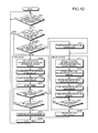
- FIG. 12 is a flowchart illustrating an example of a processing procedure of power supply control of the memory system according to the third embodiment
- FIG. 13 is a schematic view illustrating a desktop-type personal computer as an electronic device
- FIG. 14 is a schematic view illustrating a notebook-type personal computer as an electronic device
- FIG. 15 is a perspective view illustrating the external appearance of a smart phone as an electronic device.
- FIG. 16 is a perspective view illustrating the external appearance of a tablet-type terminal as an electronic device.
- a memory system includes a non-volatile first storage unit, a second storage unit, a third storage unit, and a controller.
- the controller is configured to selectively execute, following transition to a first mode, either a procedure of writing data of the second storage unit in the third storage unit, or a procedure of writing data of the third storage unit in the first storage unit while reducing power feed to the first and third storage units.
- FIG. 1 is a schematic block diagram illustrating the structure of a memory system according to a first embodiment. Constituent elements of the structure necessary for explaining the embodiment are illustrated in the drawing. Also, an instruction flow is indicated by a solid line, a power feed flow is indicated by a dotted line, and a data flow is indicated by a broken line in the drawing.
- a memory system 10 is electrically connected to a host device via an interface, such as a serial advanced technology attachment (SATA), a peripheral component interconnect express (PCIe), a serial attached small computer system interface (SAS), or a universal serial bus (USB).
- the memory system 10 functions as a storage device of a host device 20 .
- the memory system 10 receives a data access control request such as a write request, a read request, or an erase request from the host device 20 .
- Upon receiving such a data access control request the memory system 10 executes data access processing.
- An example of the memory system 10 is a solid state drive (SSD), but the memory system 10 is not limited thereto.
- the memory system 10 includes a non-volatile memory 11 as a first storage unit, a working memory 12 as a second storage unit, an operation information saving memory 13 as a third storage unit, a controller 14 , a first power supply 15 , a second power supply 16 , and a third power supply 17 .
- the non-volatile memory 11 is a storage medium capable of storing information in a non-volatile manner, with the number of times of use for storage being limited. Such a non-volatile memory 11 may be realized by, for example, a NAND-type flash memory (hereinafter referred to as a NAND memory).
- the non-volatile memory 11 stores user data and also stores management information for use in managing the memory system 10 and operation information necessary for return (hereinafter merely referred to as operation information).
- the working memory 12 stores operation information used by the controller 14 .
- the operation information may be, for example, snapshot and logs. Snapshot is, for example, data storage position management information stored at predetermined timing.
- the data storage position management information is used to manage an address designated by the host device 20 and a data storage position in the non-volatile memory 11 .
- Logs are stored as differences between data storage position management information after data contents are changed by storage of data and the snapshot. Alternatively, logs are stored as differences between a combination of the snapshot and previously acquired logs and the data storage position management information after data contents are changed by storage of data.
- the working memory 12 is formed by a volatile memory. Information stored in the working memory 12 is stored before the memory system 10 (the working memory 12 ) is turned off. Such a working memory 12 is, for example, a dynamic random access memory (DRAM) or a static RAM (SRAM).
- DRAM dynamic random access memory
- SRAM static RAM
- the operation information saving memory 13 temporarily stores the operation information stored in the working memory 12 when a condition of transition to a low power consumption mode is satisfied.
- the operation information saving memory 13 is, for example, a volatile memory such as a DRAM or an SRAM.
- the operation information stored in the operation information saving memory 13 may be stored in the non-volatile memory 11 or returned to the working memory 12 depending on a succeeding state of the memory system 10 .
- the controller 14 executes processing in the memory system 10 according to an instruction from the host device 20 .
- two stages of state are set in low power consumption mode to allow the controller 14 to execute state changing processing between the two stages of low power consumption mode and a normal state (hereinafter referred to as normal mode) by an instruction from the host device 20 or according to the state of the memory system 10 .
- the low power consumption mode includes a first state and a second state.
- the operation information is saved in the operation information saving memory 13 , and most of the power supply of the controller 14 is cut off while keeping the conduction state between the non-volatile memory 11 and the operation information saving memory 13 .
- FIG. 2 is a schematic diagram illustrating a power feed state of the memory system according to the first embodiment.
- the controller 14 is configured to execute such a switchover of the power supply and includes a memory control unit 141 , a request interpreting unit 142 , a power supply control unit 143 , and a timer 144 .
- the memory control unit 141 is configured to control a data flow and an overall behavior of the memory system 10 .
- the power supply control unit 143 receives an instruction to switch the on-off state of the first and second power supplies 15 and 16 .
- the operation information having been stored in the working memory 12 during the normal mode is saved in the operation information saving memory 13 , stored in the non-volatile memory 11 , or restored in the working memory 12 .
- transition to the first state is executed as follows.
- the operation information in the working memory 12 is saved in the operation information saving memory 13 , the timer 144 is requested to start, the request interpreting unit 142 is requested to monitor a request for return from the low power consumption mode, and the power supply control unit 143 is requested to cut off the second power supply 16 .
- Examples of the condition of transition to the low power consumption mode may include a state where the idle state having no access from the host has started, or a state where the request for transition to the low power consumption mode from the host device 20 has been issued.
- the transition to the second state is executed as follows.
- the second power supply 16 is started, the operation information in the operation information saving memory 13 is saved in the non-volatile memory 11 , the request interpreting unit 142 is requested to monitor a request for return from the low power consumption mode, and the power supply control unit 143 is requested to cut off the first and second power supplies 15 and 16 (that is, to decrease power feed from the first and second power supplies 15 and 16 to the non-volatile memory 11 and the operation information saving memory 13 ).
- An example of the condition of transition to the second state may be a state where a predetermined time has passed since the transition to the first state.
- the operation information is read from the operation information saving memory 13 to the working memory 12 , and return processing is executed.
- An example of the condition of transition to the normal mode may be a state where a request for return to the normal mode has been issued from the host device 20 .
- condition of transition to the normal mode When the condition of transition to the normal mode is satisfied in the second state, the operation information is read from the non-volatile memory 11 to the working memory 12 , and return processing is executed.
- An example of the condition of transition to the normal mode may be a state where a request for return to the normal mode has been issued from the host device 20 .
- the request interpreting unit 142 interprets the request sent from the host device 20 via an interface.
- a notification is sent to the memory control unit 141 and the power supply control unit 143 .
- the power supply control unit 143 controls cutoff or startup (on-off) of the first power supply 15 or the second power supply 16 depending on the transition state.
- the on-off switching of the first and second power supplies 15 and 16 is executed in response to a request from the memory control unit 141 .
- the on-off switching of the first and second power supplies 15 and 16 is executed in response to a request from the request interpreting unit 142 or according to a monitor result of the timer 144 .
- the power feed from the second power supply 16 to the memory control unit 141 is cut off.
- the second power supply 16 When the condition of transition to the second state of the low power consumption mode is satisfied in the first state, the second power supply 16 is turned on to store the operation information of the operation information saving memory 13 in the non-volatile memory 11 by the memory control unit 141 .
- the cutoff requests of the first and second power supplies 15 and 16 are then received from the memory control unit 141 after the operation information is stored. Accordingly, the power feed from the first power supply 15 to the non-volatile memory 11 and the operation information saving memory 13 and the power feed from the second power supply 16 to the memory control unit 141 are cut off.
- the second power supply 16 is turned on.
- the first and second power supplies 15 and 16 are turned on.
- the timer 144 starts measuring a predetermined time upon receipt of a time measurement request from the memory control unit 141 .
- time measurement is started when the condition of transition to the low power consumption mode is satisfied.
- the time measurement is executed, after the transition to the first state, to determine whether to enter the second state when no return request has been received for the predetermined time. For this purpose, an average time taken to receive the return request between the transition to the first state and the transition to the second state is previously measured, and a value larger than the average time is set as the predetermined time.
- the first power supply 15 supplies power to the non-volatile memory 11 and the operation information saving memory 13 .
- the first power supply 15 feeds power to the non-volatile memory 11 and the operation information saving memory 13 .
- the first power supply 15 cuts off power feed to the non-volatile memory 11 and the operation information saving memory 13 .
- the on-off switching of the first power supply 15 is executed by the power supply control unit 143 .
- the first power supply 15 switches on and off of the power feed to the working memory 12 , but another power supply may be used to feed power to the working memory 12 .
- the second power supply 16 feeds power to the memory control unit 141 in the controller 14 .
- power is fed to the memory control unit 141 , but the power feed to the memory control unit 141 is cut off in (the first and second states of) the low power consumption mode.
- the on-off switching of the second power supply 16 is executed by the memory control unit 141 and the power supply control unit 143 .
- the third power supply 17 feeds power to processing units in the controller 14 other than the memory control unit 141 .
- the third power supply 17 feeds power to the request interpreting unit 142 , the power supply control unit 143 , and the timer 144 .
- the third power supply 17 feeds power to the request interpreting unit 142 , the power supply control unit 143 , and the timer 144 in the normal state and in the low power consumption mode as well.
- FIG. 3 is a flowchart illustrating an example of a processing procedure of power supply control in the memory system according to the first embodiment. It is assumed herein that the first to third power supplies 15 to 17 are used in the normal mode where all power supplies are turned on (step S 11 ). In this state, it is determined whether the low power consumption mode transition condition is satisfied (step S 12 ). Examples of the condition of transition to the low power consumption mode may include a state where the idle state has started in the memory system 10 , or a state where the request for transition to the low power consumption mode from the host device 20 has been issued.
- step S 12 When the low power consumption mode transition condition is not satisfied (No at step S 12 ), the process returns to step S 11 and the use in the normal mode is started.
- step S 12 when the low power consumption mode transition condition is satisfied (Yes at step S 12 ), the operation enters the first state of the low power consumption mode.
- the operation information stored in the working memory 12 is saved in the operation information saving memory 13 (step S 13 ), and the power feed from the second power supply 16 to the controller 14 is cut off (step S 14 ).
- the timer 144 is set (step S 15 ), and the time measurement for a predetermined time is started.
- step S 16 it is determined whether a predetermined time has passed. If the predetermined time has not passed (No at step S 16 ), it is determined whether a return request is received from the host device 20 (step S 17 ). If no return request has been received (No at step S 17 ), the process returns to step S 16 .
- step S 17 if the return request has been received from the host device 20 (Yes at step S 17 ), cancellation processing of the low power consumption mode is executed. Specifically, the power feed from the second power supply 16 to the controller 14 is turned on (step S 18 ), and the operation information having been saved temporarily in the operation information saving memory 13 is read to the working memory 12 (step S 19 ). Accordingly, the use in the normal mode is executed (step S 29 ), and the processing is ended.
- step S 16 When the predetermined time has passed in step S 16 (Yes at step S 16 ), that is, when the predetermined time has passed before the return request is received from the host device 20 , the power feed from the second power supply 16 to the controller 14 is turned on (step S 20 ). The second state of the low power consumption mode is thus entered.
- the power feed to the controller 14 aims to execute information storing processing of the operation information from the operation information saving memory 13 to the non-volatile memory 11 before entering the second state.
- the operation information is read from the operation information saving memory 13 (step S 21 ), and the read operation information is saved in the non-volatile memory 11 (step S 22 ).
- the power feed from the second power supply 16 to the controller 14 is turned off (step S 23 ), and the power feed from the first power supply 15 to the non-volatile memory 11 and the operation information saving memory 13 is also turned off (step S 24 ).
- step S 25 it is determined whether the return request has been received from the host device 20 (step S 25 ). If no return request has been received (No at step S 25 ), the process enters a wait state until the return request is received (step S 25 ).
- step S 25 the cancellation processing of the low power consumption mode is executed. Specifically, the power feed from the first power supply 15 to the non-volatile memory 11 and the operation information saving memory 13 is turned on (step S 26 ), the power feed from the second power supply 16 to the controller 14 is turned on (step S 27 ), and the latest operation information saved in the non-volatile memory 11 is read to the working memory 12 (step S 28 ). Accordingly, the use in the normal mode is executed (step S 29 ), and the processing is ended.
- Such operations include transition processing from the normal mode to the first state of the low power consumption mode, processing in the first state, transition processing from the first state to the normal mode, transition processing from the first state to the second state, processing in the second state, and transition processing from the second state to the normal mode.
- FIG. 4 is a flowchart illustrating an example of a procedure of the memory control unit in transition processing from the normal mode to the first state of the low power consumption mode.
- the memory control unit 141 temporarily saves, in the operation information saving memory 13 , the operation information including the management information necessary for the operation of the memory system 10 and the return information necessary for return (step S 52 ).
- the memory control unit 141 issues a request to start counting to the timer 144 (step S 53 ), a request to monitor the request from the host device 20 to the request interpreting unit 142 (step S 54 ), and a cutoff request to the power supply control unit 143 to turn off the second power supply 16 (step S 55 ). Accordingly, the transition processing to the first state by the memory control unit 141 is ended.
- FIG. 5 is a flowchart illustrating an example of a processing procedure in the first state of the power supply control unit and the timer.
- the timer 144 receives the request to start counting from the memory control unit 141 in step S 53 of FIG. 4 (step S 73 ) and starts counting (step S 74 ).
- the power supply control unit 143 determines whether the request for return from the low power consumption mode has been received from the request interpreting unit 142 (step S 75 ).
- the return request is issued from the host device 20 and monitored by the request interpreting unit 142 .
- the predetermined time has not passed yet (No at step S 76 )
- the process returns to step S 75 .
- the power supply control unit 143 executes the transition processing to the second state (step S 77 ), and the processing of the power supply control unit 143 and the timer 144 in the first state is ended.
- the predetermined time to be measured by the timer 144 is determined based on, for example, the possible number of times the non-volatile memory 11 is rewritten, or an estimated number of times the memory system 10 would enter the low power consumption mode in the environment of use.
- step S 75 When the return request is received from the request interpreting unit 142 in step S 75 (Yes at step S 75 ), the power supply control unit 143 executes return processing from the low power consumption mode to the normal mode (step S 78 ), whereby the processing of the power supply control unit 143 and the timer 144 in the first state is ended.
- FIG. 6 is a flowchart illustrating an example of a transition processing procedure from the first state to the normal mode.
- step S 75 of FIG. 5 when the power supply control unit 143 receives, from the request interpreting unit 142 , the request for return from the low power consumption mode (step S 91 ), the second power supply 16 is turned on to place the memory control unit 141 in an operation state (step S 92 ). Accordingly, the memory control unit 141 becomes operable.
- the memory control unit 141 reads the operation information from the operation information saving memory 13 (step S 93 ), and executes return processing by storing the read operation information in the working memory 12 (step S 94 ). Accordingly, the return processing is complete.
- FIG. 7 is a flowchart illustrating an example of a transition processing procedure from the first state to the second state in the power supply control unit and the memory control unit.
- the memory control unit 141 reads the operation information temporarily saved in the operation information saving memory 13 in step S 52 of FIG. 4 and stores the read operation information in the non-volatile memory 11 (step S 113 ). After that, the memory control unit 141 requests the request interpreting unit 142 to monitor the request for return from the low power consumption mode (step S 114 ), while issuing the cutoff request to the power supply control unit 143 to cut off power feed to the first power supply 15 and the second power supply 16 (step S 115 ). Thus, the transition processing to the second state is complete.
- FIG. 8 is a flowchart illustrating an example of an operation processing procedure of the power supply control unit in the second state.
- the power supply control unit 143 cuts them off (step S 132 ). Accordingly, the power feed to the memory control unit 141 , the non-volatile memory 11 , and the operation information saving memory 13 is cut off.
- a wait state is entered until the cancellation request is received.
- step S 133 When the request to cancel the low power consumption mode has been received (Yes at step S 133 ), the return processing to the normal mode is executed (step S 134 ). Accordingly, the processing of the power supply control unit 143 in the second state is ended.
- FIG. 9 is a flowchart illustrating an example of a transition processing procedure from the second state to the normal mode.
- the memory control unit 141 then reads the latest operation information from the non-volatile memory 11 (step S 153 ), and stores the read operation information in the working memory 12 to execute the return processing (step S 154 ). Accordingly, a transition to the normal mode is complete and the return processing from the second state is ended.
- the first to third power supplies 15 to 17 are provided to feed power separately to a group including the request interpreting unit 142 , the power supply control unit 143 , and the timer 144 , the memory control unit 141 , and a group including the non-volatile memory 11 , and the operation information saving memory 13 .
- the first and second states are provided in the low power consumption mode. In the first state, when the request to enter the low power consumption mode is received, the operation information in the working memory 12 is temporarily saved in the operation information saving memory 13 , and the second power supply 16 is turned off.
- the operation information having been saved in the operation information saving memory 13 is stored in the non-volatile memory 11 before the first and second power supplies 15 and 16 are turned off.
- the request for transition to the low power consumption mode is issued, if the request for return to the normal mode is issued within the predetermined time, the return processing from the first state where the operation information has not been stored yet in the non-volatile memory 11 can be executed.
- the power consumption can be decreased compared to that of the related art, the number of rewriting times of the non-volatile memory 11 having a limited number of rewriting times is decreased, and the lifetime of the non-volatile memory 11 can be extended.
- the first state is maintained within the predetermined time, followed by entering the second state.
- the power feed to the operation information saving memory 13 formed by a volatile memory is not increased more than needed.
- the second power supply 16 since the second power supply 16 has been turned off in the first state, the power consumption can be decreased compared to the normal mode.
- the memory system 10 has a structure similar to that of the first embodiment illustrated in FIG. 1 .
- the memory control unit 141 starts the timer 144 at the time of the initial startup or returning from the low power consumption mode.
- the memory control unit 141 determines whether the memory system 10 should be placed in the first state or the second state of the low power consumption mode, depending on whether a predetermined time has passed.
- the memory control unit 141 executes the control according to the result of determination.
- Other constituent elements are similar to those described in the first embodiment, and the description thereof will not be repeated.
- FIG. 10 is a flowchart illustrating an example of a processing procedure of the power supply control in the memory system according to the second embodiment.
- the memory control unit 141 starts the timer 144 in response to the transition to the normal mode (step S 171 ).
- the length of time to be measured by the timer 144 may be, for example, longer (but not long enough to enter the second state when entering the loop) than the time needed between the return request and the transition request in the case where the memory system 10 enters a loop of repeating requests for transition to the low power consumption mode and requests for return to the normal mode.
- the memory control unit 141 determines whether the low power consumption mode transition condition is satisfied (step S 172 ). When the low power consumption mode transition condition is not satisfied (No at step S 172 ), a wait state is entered until the low power consumption mode transition condition is satisfied.
- step S 173 it is determined whether a predetermined time has passed since the start of the timer 144 (step S 173 ). If the predetermined time has not passed yet since the start of the timer 144 (No at step S 173 ), the transition processing to the first state of the low power consumption mode is executed similarly to that described in steps S 13 to S 17 of FIG. 3 (steps S 174 to S 178 ).
- step S 179 first return processing from the low power consumption mode to the normal mode is executed.
- the power feed from the second power supply 16 to the controller 14 is turned on, and the operation information having been saved temporarily in the operation information saving memory 13 is read to the working memory 12 . Accordingly, the use in the normal mode is started.
- the memory control unit 141 starts the timer 144 (step S 187 ), and the process returns to step S 172 .
- step S 173 when the predetermined time has passed since the start of the timer 144 (Yes at step S 173 ), the transition processing to the second state of the low power consumption mode is executed similarly to that described in steps S 21 to S 25 of FIG. 3 (steps S 181 to S 185 ).
- step S 177 when the predetermined time has passed in the first state since the start of the timer 144 (Yes at step S 177 ), or when the predetermined time has passed before the return request is received from the host device 20 , the power feed from the second power supply 16 to the controller 14 is turned on (step S 180 ) to enter the second state of the low power consumption mode (steps S 181 to 185 ).
- step S 186 the second return processing from the low power consumption mode to the normal mode is executed.
- the power feed from the first power supply 15 to the non-volatile memory 11 and the operation information saving memory 13 is turned on
- the power feed from the second power supply 16 to the controller 14 is turned on
- the latest operation information saved in the non-volatile memory 11 is read to the working memory 12 . Accordingly, the use in the normal mode is started.
- the memory control unit 141 starts the timer 144 (step S 187 ), and the process returns to step S 172 .
- the timer 144 configured to measure the predetermined time is set. After that, when the low power consumption mode transition condition is satisfied, the state of the low power consumption mode is changed depending on whether the timer 144 has measured the predetermined time or more. Specifically, if the request for transition to the low power consumption mode is received before the predetermined time has passed, it is highly probable to receive the return request soon. Therefore, the first state in which the return processing can be executed immediately is entered. When the request for transition to the low power consumption mode is received after the predetermined time has passed, the second state is entered, as it is less probable to receive the return request thereafter.
- the first state can be entered to prevent useless storage of the operation information in the non-volatile memory 11 . Accordingly, the number of times the non-volatile memory 11 is rewritten can be decreased, to extend the lifetime of the non-volatile memory 11 .
- FIG. 11 is a schematic block diagram illustrating the structure of the memory system according to the third embodiment. Again, constituent elements of the structure necessary for explaining the embodiment are illustrated in the drawing. Also, the instruction flow is indicated by a solid line, the power feed flow is indicated by a dotted line, and the data flow is indicated by a broken line in the drawing.
- the memory system 10 has a structure similar to that according to the first embodiment illustrated in FIG. 1 , and further includes a state storage unit 145 .
- the state storage unit 145 stores the final state of the last mode indicating the first state or the second state, when the transition to the low power consumption mode has been executed.
- the final state of the last mode is referenced when the mode is returned from the low power consumption mode to the normal mode.
- the memory control unit 141 switches the transition between two states according to the final state of the last low power consumption mode. Specifically, when the final state of the last low power consumption mode, that is, the final state of the last mode stored in the state storage unit 145 is the first state, the first state is entered. When the final state of the last mode is the second state and the low power consumption mode transition condition is satisfied before the predetermined time has passed since the last return processing, the first state is entered again. When the final state of the last mode is the second state and the low power consumption mode transition condition is satisfied with the predetermined time having passed since the last return processing, the second state is entered.
- FIG. 12 is a flowchart illustrating an example of a processing procedure of power supply control of the memory system according to the third embodiment. First, it is assumed that the memory system 10 is in the normal mode, and that the timer 144 configured to measure a predetermined time during the return processing to the normal mode has been started.
- the memory control unit 141 determines whether the low power consumption mode transition condition is satisfied (step S 201 ). When the low power consumption mode transition condition has not been satisfied (No in step S 201 ), the wait state is entered until the low power consumption mode transition condition is satisfied. When the low power consumption mode transition condition has been satisfied (Yes at step S 201 ), the memory control unit 141 obtains, from the state storage unit 145 , information as to whether the final state of the last low power consumption mode has been the first state or the second state (step S 202 ).
- step S 202 when the final state of the last mode has been the second state, it is determined whether the low power consumption mode transition condition has been satisfied after the predetermined time has passed from the last return (step S 203 ). Since the timer 144 has already been started when the return processing to the last normal mode is executed, as described above, the determination can be done simply by reading the time of the timer 144 . As described in the second embodiment, the predetermined time may be, for example, longer than the time between the return request and the transition request when the memory system 10 has entered a loop of repeating requests for transition to the low power consumption mode and requests for return to the normal mode (but not long enough to enter the second state when the loop is entered).
- step S 204 the transition processing from the normal mode to the first state of the low power consumption mode is executed (steps S 204 to S 209 ).
- This transition processing to the first state is mostly similar to that described at steps S 13 to S 17 of FIG. 3 , but the processing also includes processing (step S 205 ) of storing the current state of the low power consumption mode, that is, the first state in the state storage unit 145 before the controller 14 is turned off.
- step S 210 the first return processing to the normal mode from the low power consumption mode is executed.
- the power feed from the second power supply 16 to the controller 14 is turned on, and the operation information having been saved temporarily in the operation information saving memory 13 is read to the working memory 12 . Accordingly, the use in the normal mode is started.
- the memory control unit 141 starts the timer 144 (step S 219 ). The time measured by the timer 144 is used, when the low power consumption mode transition condition is satisfied, in determining whether the predetermined time has passed since the last return in step S 203 . Subsequently, the process returns to step S 201 .
- step S 203 when the predetermined time has passed after the timer 144 is started (Yes at step S 203 ), the transition processing to the second state of the low power consumption mode is executed (steps S 212 to S 217 ).
- This transition processing to the second state is mostly similar to that described at steps S 21 to S 25 of FIG. 3 , but the processing also includes storing the current state of the low power consumption mode, that is, the second state in the state storage unit 145 before the controller 14 is turned off (step S 214 ).
- step S 208 When the predetermined time has passed in the first state since the startup of the timer 144 (Yes at step S 208 ), that is, when the predetermined time has passed before the return request is received from the host device 20 , the power feed from the second power supply 16 to the controller 14 is turned on (step S 211 ) to enter the second state of the low power consumption mode (steps S 212 to S 217 ).
- step S 218 the second return processing from the low power consumption mode to the normal mode is executed (step S 218 ).
- the second return processing as described in steps S 26 to S 29 of FIG. 3 , the power feed from the first power supply 15 to the non-volatile memory 11 and the operation information saving memory 13 is turned on, the power feed from the second power supply 16 to the controller 14 is turned on, and the latest operation information saved in the non-volatile memory 11 is read to the working memory 12 .
- the memory control unit 141 starts the timer 144 (step S 219 ), and the process returns to step S 201 .
- the state of the mode is stored. After setting the timer 144 to measure the predetermined time in returning to the normal mode, the state corresponding to the final state of the last mode can be entered when the low power consumption mode transition condition is satisfied. Accordingly, if the entry and return to and from the low power consumption mode occur in a short time, it is determined that the system is placed in a short-cycled loop, and the operation information is temporarily saved in the operation information saving memory 13 . Accordingly, the number of times the non-volatile memory 11 is rewritten can be decreased.
- two stages of state have been set in the low power consumption mode, but the embodiments are not limited thereto.
- three or more stages of state may be provided in the low power consumption mode by dividing the memory control unit 141 into several regions and controlling each region by separate power supply.
- the state of the low power consumption mode may be further divided by providing separate power supplies for the non-volatile memory 11 and the operation information saving memory 13 . By doing this, the power consumption can be controlled more finely.
- the memory system described in the first to third embodiments above can be applied to electronic devices.
- the electronic devices having the memory systems of the first to third embodiments applied thereto will be described.
- FIG. 13 is a schematic view illustrating a desktop-type personal computer as an electronic device.
- a desktop-type personal computer 100 includes a body 110 , a display 120 , a keyboard 121 , a mouse 122 , etc.
- the body 110 includes a mother board 111 , on which major hardware is installed, a memory system 10 , a power supply device 113 , etc.
- the memory system 10 is physically connected to the mother board 111 via a SATA cable, and further connected electrically to a CPU mounted on the mother board 111 via a southbridge mounted thereon.
- the power supply device 113 generates various types of power for use in the desktop-type personal computer 100 , and supplies power to the mother board ill, the memory system 10 , etc., via a power supply cable.
- FIG. 14 is a schematic view illustrating a notebook-type personal computer as an electronic device.
- a notebook-type personal computer 200 includes a body 210 , a display unit 221 , etc.
- the display unit 221 incorporates a display device 220 formed by, for example, a liquid crystal display (LCD).
- the display unit 221 is attached to the body 210 to be rotatable between an open position where the top surface of the body 210 is exposed and a close position where the display unit 221 covers the top surface of the body 210 .
- the body 210 has a thin box-like housing, with a power supply switch 211 , a keyboard 212 , a touch pad 213 , etc. arranged on the top surface thereof. Similar to the desktop-type personal computer 100 , the body 210 also includes the memory system 10 , a mother board, a power supply device, etc.
- FIG. 15 is a perspective view illustrating an external appearance of a smart phone as an electronic device.
- a smart phone 300 includes a body 310 and a touch screen display 320 .
- the body 310 has a thin box-like housing.
- the touch screen display 320 incorporates an LCD and a touch panel.
- the touch panel is provided to cover the LCD screen.
- the touch screen display 320 is overlaid on the top surface of the body 310 .
- a power button 311 configured to turn on/off the power supply of the smart phone 300 , a volume control button 312 , etc. are arranged.
- a speaker 313 and other constituent elements are arranged in the vicinity of the upper part of the top surface of the body 310 .
- a micro-universal serial bus (micro USB) connector which is not illustrated, for use in connecting a USB cable or a USB device, for example, of the USB 2.0 standard is arranged.
- SoC system on a chip
- the SoC is connected to the main memory, the memory system, etc. via wiring.
- FIG. 16 is a perspective view illustrating an external appearance of a tablet-type terminal as an electronic device.
- the structure of a tablet terminal 400 is mostly similar to that of the smart phone 300 of FIG. 15 , except for the size of a touch screen display 420 .
- a typical size of the touch screen display 320 of the smart phone 300 is 5 inches or smaller, while the touch screen display 420 of the tablet terminal 400 is usually larger than 5 inches.
- a power button On the side of the body 410 , there are provided a power button, a volume control button, a speaker, a memory card slot, a USB connector 411 , an external display connecting terminal 412 compatible with a high-definition multimedia interface (HDMI) standard, etc.
- the external display connecting terminal 412 is provided for use in supplying an output of a digital video signal to an external display.
- the internal structure of the body 410 is similar to that of the smart phone 300 of FIG. 15 .
- the desktop-type personal computer 100 the notebook-type personal computer 200 , the smart phone 300 , and the tablet terminal 400 have been described as examples of the electronic devices in the above description, the electronic devices are not limited to those devices and may include a PDA, an image capturing device such as a still camera or a video camera, a game console, and a car navigation system.
Abstract
Description
Claims (20)
Priority Applications (1)
| Application Number | Priority Date | Filing Date | Title |
|---|---|---|---|
| US14/302,835 US9442560B2 (en) | 2014-02-26 | 2014-06-12 | Memory system minimizing occurrences of storing of operation data in non-volatile storage during power saving mode |
Applications Claiming Priority (2)
| Application Number | Priority Date | Filing Date | Title |
|---|---|---|---|
| US201461944867P | 2014-02-26 | 2014-02-26 | |
| US14/302,835 US9442560B2 (en) | 2014-02-26 | 2014-06-12 | Memory system minimizing occurrences of storing of operation data in non-volatile storage during power saving mode |
Publications (2)
| Publication Number | Publication Date |
|---|---|
| US20150241952A1 US20150241952A1 (en) | 2015-08-27 |
| US9442560B2 true US9442560B2 (en) | 2016-09-13 |
Family
ID=53882160
Family Applications (1)
| Application Number | Title | Priority Date | Filing Date |
|---|---|---|---|
| US14/302,835 Active 2034-11-13 US9442560B2 (en) | 2014-02-26 | 2014-06-12 | Memory system minimizing occurrences of storing of operation data in non-volatile storage during power saving mode |
Country Status (1)
| Country | Link |
|---|---|
| US (1) | US9442560B2 (en) |
Cited By (1)
| Publication number | Priority date | Publication date | Assignee | Title |
|---|---|---|---|---|
| US20160266638A1 (en) * | 2015-03-10 | 2016-09-15 | Kabushiki Kaisha Toshiba | Memory system, method of controlling memory system having volatile memory and nonvolatile memory, and controller |
Families Citing this family (6)
| Publication number | Priority date | Publication date | Assignee | Title |
|---|---|---|---|---|
| DE112015002911T5 (en) * | 2014-06-20 | 2017-03-09 | Semiconductor Energy Laboratory Co., Ltd. | Semiconductor device |
| US10007319B2 (en) * | 2015-12-17 | 2018-06-26 | Microsemi Solutions (U.S.), Inc. | Power saving in multi-directional data transfer |
| US11561603B2 (en) * | 2018-12-20 | 2023-01-24 | Micron Technology, Inc. | Memory device low power mode |
| US20200388319A1 (en) | 2019-06-07 | 2020-12-10 | Semiconductor Energy Laboratory Co., Ltd. | Semiconductor device, electronic component, and electronic device |
| US11934252B2 (en) | 2021-03-17 | 2024-03-19 | Micron Technology, Inc. | Shallow hibernate power state |
| JP2023040578A (en) * | 2021-09-10 | 2023-03-23 | キオクシア株式会社 | Memory system and control method |
Citations (14)
| Publication number | Priority date | Publication date | Assignee | Title |
|---|---|---|---|---|
| US5414861A (en) | 1991-09-11 | 1995-05-09 | Fujitsu Limited | Data protection system using different levels of reserve power to maintain data in volatile memories for any period of time |
| JPH11184569A (en) | 1997-12-25 | 1999-07-09 | Fujitsu Denso Ltd | Data backup device and data backup method for semiconductor memory |
| US20060171231A1 (en) * | 2005-01-31 | 2006-08-03 | Song Ho U | Memory device |
| US20090024843A1 (en) * | 2007-07-19 | 2009-01-22 | Choi Byung Yoon | Computer having flash memory and method of operating flash memory |
| US20090172439A1 (en) * | 2007-12-28 | 2009-07-02 | Intel Corporation | System and method for fast platform hibernate and resume |
| JP2009237602A (en) | 2008-03-25 | 2009-10-15 | Toshiba Memory Systems Co Ltd | Memory system |
| US20100169687A1 (en) * | 2008-12-26 | 2010-07-01 | Kabushiki Kaisha Toshiba | Data storage device and power-saving control method for data storage device |
| US20110078463A1 (en) * | 2009-09-25 | 2011-03-31 | Fleming Bruce L | Method, system and apparatus for low-power storage of processor context information |
| US20120079171A1 (en) * | 2010-09-29 | 2012-03-29 | Samsung Electronics Co., Ltd. | Non-volatile memory systems and methods of managing power of the same |
| US20120159060A1 (en) | 2010-12-20 | 2012-06-21 | James Yu | Power isolation for memory backup |
| US8438348B2 (en) | 2008-03-27 | 2013-05-07 | Hitachi, Ltd. | Disk array device |
| US20140040650A1 (en) | 2012-07-31 | 2014-02-06 | Toshikatsu Hida | Semiconductor storage device and method for controlling the semiconductor storage device |
| US20140281599A1 (en) * | 2013-03-14 | 2014-09-18 | Knut S. Grimsrud | Nand page buffer based volatile state store |
| US20150178009A1 (en) * | 2013-12-24 | 2015-06-25 | SK Hynix Inc. | Data storage device and data processing system including the same |
-
2014
- 2014-06-12 US US14/302,835 patent/US9442560B2/en active Active
Patent Citations (14)
| Publication number | Priority date | Publication date | Assignee | Title |
|---|---|---|---|---|
| US5414861A (en) | 1991-09-11 | 1995-05-09 | Fujitsu Limited | Data protection system using different levels of reserve power to maintain data in volatile memories for any period of time |
| JPH11184569A (en) | 1997-12-25 | 1999-07-09 | Fujitsu Denso Ltd | Data backup device and data backup method for semiconductor memory |
| US20060171231A1 (en) * | 2005-01-31 | 2006-08-03 | Song Ho U | Memory device |
| US20090024843A1 (en) * | 2007-07-19 | 2009-01-22 | Choi Byung Yoon | Computer having flash memory and method of operating flash memory |
| US20090172439A1 (en) * | 2007-12-28 | 2009-07-02 | Intel Corporation | System and method for fast platform hibernate and resume |
| JP2009237602A (en) | 2008-03-25 | 2009-10-15 | Toshiba Memory Systems Co Ltd | Memory system |
| US8438348B2 (en) | 2008-03-27 | 2013-05-07 | Hitachi, Ltd. | Disk array device |
| US20100169687A1 (en) * | 2008-12-26 | 2010-07-01 | Kabushiki Kaisha Toshiba | Data storage device and power-saving control method for data storage device |
| US20110078463A1 (en) * | 2009-09-25 | 2011-03-31 | Fleming Bruce L | Method, system and apparatus for low-power storage of processor context information |
| US20120079171A1 (en) * | 2010-09-29 | 2012-03-29 | Samsung Electronics Co., Ltd. | Non-volatile memory systems and methods of managing power of the same |
| US20120159060A1 (en) | 2010-12-20 | 2012-06-21 | James Yu | Power isolation for memory backup |
| US20140040650A1 (en) | 2012-07-31 | 2014-02-06 | Toshikatsu Hida | Semiconductor storage device and method for controlling the semiconductor storage device |
| US20140281599A1 (en) * | 2013-03-14 | 2014-09-18 | Knut S. Grimsrud | Nand page buffer based volatile state store |
| US20150178009A1 (en) * | 2013-12-24 | 2015-06-25 | SK Hynix Inc. | Data storage device and data processing system including the same |
Non-Patent Citations (1)
| Title |
|---|
| U.S. Appl. No. 14/796,330, filed Jul. 10, 2015, Anazawa, et al. |
Cited By (2)
| Publication number | Priority date | Publication date | Assignee | Title |
|---|---|---|---|---|
| US20160266638A1 (en) * | 2015-03-10 | 2016-09-15 | Kabushiki Kaisha Toshiba | Memory system, method of controlling memory system having volatile memory and nonvolatile memory, and controller |
| US9568987B2 (en) * | 2015-03-10 | 2017-02-14 | Kabushiki Kaisha Toshiba | Memory system, method of controlling memory system having volatile memory and nonvolatile memory, and controller |
Also Published As
| Publication number | Publication date |
|---|---|
| US20150241952A1 (en) | 2015-08-27 |
Similar Documents
| Publication | Publication Date | Title |
|---|---|---|
| US9442560B2 (en) | Memory system minimizing occurrences of storing of operation data in non-volatile storage during power saving mode | |
| US11372472B2 (en) | System on chip for reducing wake-up time, method of operating same, and computer system including same | |
| US7913073B2 (en) | System embedding plural controller sharing nonvolatile memory | |
| US8151036B2 (en) | Memory controller, memory system, and access control method of flash memory | |
| US9606920B2 (en) | Multi-CPU system and computing system having the same | |
| US9092150B2 (en) | Systems and methods of performing a data save operation | |
| US8970884B2 (en) | Image forming apparatus | |
| US8914594B2 (en) | Systems and methods of loading data from a non-volatile memory to a volatile memory | |
| US9032235B2 (en) | Semiconductor storage device and method for controlling the semiconductor storage device | |
| US7979687B2 (en) | Quick start | |
| US20060245274A1 (en) | Apparatus and method for controlling NAND flash memory | |
| US9575663B2 (en) | Solid state drive and operation method thereof | |
| US8769319B2 (en) | Reducing power consumption in memory line architecture | |
| KR20180092435A (en) | Data storage device and operating method thereof | |
| JP2014016782A (en) | Information processing device and program | |
| EP3573063B1 (en) | Power-down/power-loss memory controller | |
| US20170038974A1 (en) | Storage device changing condition parameter value based on aging level and method for managing the same | |
| KR20190093400A (en) | Semiconductor memory device and electronic device including the same | |
| CN111459527A (en) | Memory system and operating method thereof | |
| US20140292776A1 (en) | Electronic apparatus and control method | |
| US20210303432A1 (en) | Computer program product and method and apparatus for controlling access to flash memory card | |
| CN108417232B (en) | Data storage device and operation method thereof | |
| KR20150106144A (en) | Method for controlling memory swap operation and data processing system adopting the same | |
| US20160313942A1 (en) | Electronic apparatus, method, and computer readable medium | |
| US20240004578A1 (en) | Memory system and method of operating memory controller included in the memory system |
Legal Events
| Date | Code | Title | Description |
|---|---|---|---|
| AS | Assignment |
Owner name: KABUSHIKI KAISHA TOSHIBA, JAPAN Free format text: ASSIGNMENT OF ASSIGNORS INTEREST;ASSIGNORS:ASAMI, SHOHEI;HIDA, TOSHIKATSU;TADOKORO, MITSUNORI;AND OTHERS;REEL/FRAME:033090/0314 Effective date: 20140605 |
|
| STCF | Information on status: patent grant |
Free format text: PATENTED CASE |
|
| AS | Assignment |
Owner name: TOSHIBA MEMORY CORPORATION, JAPAN Free format text: ASSIGNMENT OF ASSIGNORS INTEREST;ASSIGNOR:KABUSHIKI KAISHA TOSHIBA;REEL/FRAME:043709/0035 Effective date: 20170706 |
|
| MAFP | Maintenance fee payment |
Free format text: PAYMENT OF MAINTENANCE FEE, 4TH YEAR, LARGE ENTITY (ORIGINAL EVENT CODE: M1551); ENTITY STATUS OF PATENT OWNER: LARGE ENTITY Year of fee payment: 4 |
|
| AS | Assignment |
Owner name: K.K. PANGEA, JAPAN Free format text: MERGER;ASSIGNOR:TOSHIBA MEMORY CORPORATION;REEL/FRAME:055659/0471 Effective date: 20180801 Owner name: KIOXIA CORPORATION, JAPAN Free format text: CHANGE OF NAME AND ADDRESS;ASSIGNOR:TOSHIBA MEMORY CORPORATION;REEL/FRAME:055669/0001 Effective date: 20191001 Owner name: TOSHIBA MEMORY CORPORATION, JAPAN Free format text: CHANGE OF NAME AND ADDRESS;ASSIGNOR:K.K. PANGEA;REEL/FRAME:055669/0401 Effective date: 20180801 |
|
| MAFP | Maintenance fee payment |
Free format text: PAYMENT OF MAINTENANCE FEE, 8TH YEAR, LARGE ENTITY (ORIGINAL EVENT CODE: M1552); ENTITY STATUS OF PATENT OWNER: LARGE ENTITY Year of fee payment: 8 |