US9483339B2 - Systems and methods for fast bit error rate estimation - Google Patents
Systems and methods for fast bit error rate estimation Download PDFInfo
- Publication number
- US9483339B2 US9483339B2 US14/318,310 US201414318310A US9483339B2 US 9483339 B2 US9483339 B2 US 9483339B2 US 201414318310 A US201414318310 A US 201414318310A US 9483339 B2 US9483339 B2 US 9483339B2
- Authority
- US
- United States
- Prior art keywords
- data
- memory
- memory cells
- error rate
- read
- Prior art date
- Legal status (The legal status is an assumption and is not a legal conclusion. Google has not performed a legal analysis and makes no representation as to the accuracy of the status listed.)
- Active, expires
Links
Images


Classifications
-
- G—PHYSICS
- G06—COMPUTING; CALCULATING OR COUNTING
- G06F—ELECTRIC DIGITAL DATA PROCESSING
- G06F11/00—Error detection; Error correction; Monitoring
- G06F11/07—Responding to the occurrence of a fault, e.g. fault tolerance
- G06F11/0703—Error or fault processing not based on redundancy, i.e. by taking additional measures to deal with the error or fault not making use of redundancy in operation, in hardware, or in data representation
- G06F11/0751—Error or fault detection not based on redundancy
- G06F11/0754—Error or fault detection not based on redundancy by exceeding limits
- G06F11/076—Error or fault detection not based on redundancy by exceeding limits by exceeding a count or rate limit, e.g. word- or bit count limit
-
- G—PHYSICS
- G06—COMPUTING; CALCULATING OR COUNTING
- G06F—ELECTRIC DIGITAL DATA PROCESSING
- G06F12/00—Accessing, addressing or allocating within memory systems or architectures
- G06F12/02—Addressing or allocation; Relocation
- G06F12/0223—User address space allocation, e.g. contiguous or non contiguous base addressing
- G06F12/023—Free address space management
- G06F12/0238—Memory management in non-volatile memory, e.g. resistive RAM or ferroelectric memory
- G06F12/0246—Memory management in non-volatile memory, e.g. resistive RAM or ferroelectric memory in block erasable memory, e.g. flash memory
-
- G—PHYSICS
- G06—COMPUTING; CALCULATING OR COUNTING
- G06F—ELECTRIC DIGITAL DATA PROCESSING
- G06F11/00—Error detection; Error correction; Monitoring
- G06F11/07—Responding to the occurrence of a fault, e.g. fault tolerance
- G06F11/08—Error detection or correction by redundancy in data representation, e.g. by using checking codes
- G06F11/10—Adding special bits or symbols to the coded information, e.g. parity check, casting out 9's or 11's
- G06F11/1004—Adding special bits or symbols to the coded information, e.g. parity check, casting out 9's or 11's to protect a block of data words, e.g. CRC or checksum
-
- G—PHYSICS
- G06—COMPUTING; CALCULATING OR COUNTING
- G06F—ELECTRIC DIGITAL DATA PROCESSING
- G06F11/00—Error detection; Error correction; Monitoring
- G06F11/07—Responding to the occurrence of a fault, e.g. fault tolerance
- G06F11/08—Error detection or correction by redundancy in data representation, e.g. by using checking codes
- G06F11/10—Adding special bits or symbols to the coded information, e.g. parity check, casting out 9's or 11's
- G06F11/1008—Adding special bits or symbols to the coded information, e.g. parity check, casting out 9's or 11's in individual solid state devices
- G06F11/1048—Adding special bits or symbols to the coded information, e.g. parity check, casting out 9's or 11's in individual solid state devices using arrangements adapted for a specific error detection or correction feature
-
- G—PHYSICS
- G06—COMPUTING; CALCULATING OR COUNTING
- G06F—ELECTRIC DIGITAL DATA PROCESSING
- G06F11/00—Error detection; Error correction; Monitoring
- G06F11/07—Responding to the occurrence of a fault, e.g. fault tolerance
- G06F11/08—Error detection or correction by redundancy in data representation, e.g. by using checking codes
- G06F11/10—Adding special bits or symbols to the coded information, e.g. parity check, casting out 9's or 11's
- G06F11/1008—Adding special bits or symbols to the coded information, e.g. parity check, casting out 9's or 11's in individual solid state devices
- G06F11/1068—Adding special bits or symbols to the coded information, e.g. parity check, casting out 9's or 11's in individual solid state devices in sector programmable memories, e.g. flash disk
-
- G—PHYSICS
- G11—INFORMATION STORAGE
- G11C—STATIC STORES
- G11C11/00—Digital stores characterised by the use of particular electric or magnetic storage elements; Storage elements therefor
- G11C11/56—Digital stores characterised by the use of particular electric or magnetic storage elements; Storage elements therefor using storage elements with more than two stable states represented by steps, e.g. of voltage, current, phase, frequency
- G11C11/5621—Digital stores characterised by the use of particular electric or magnetic storage elements; Storage elements therefor using storage elements with more than two stable states represented by steps, e.g. of voltage, current, phase, frequency using charge storage in a floating gate
- G11C11/5628—Programming or writing circuits; Data input circuits
-
- G—PHYSICS
- G11—INFORMATION STORAGE
- G11C—STATIC STORES
- G11C16/00—Erasable programmable read-only memories
- G11C16/02—Erasable programmable read-only memories electrically programmable
- G11C16/06—Auxiliary circuits, e.g. for writing into memory
- G11C16/34—Determination of programming status, e.g. threshold voltage, overprogramming or underprogramming, retention
- G11C16/3436—Arrangements for verifying correct programming or erasure
- G11C16/3454—Arrangements for verifying correct programming or for detecting overprogrammed cells
- G11C16/3459—Circuits or methods to verify correct programming of nonvolatile memory cells
-
- G—PHYSICS
- G11—INFORMATION STORAGE
- G11C—STATIC STORES
- G11C16/00—Erasable programmable read-only memories
- G11C16/02—Erasable programmable read-only memories electrically programmable
- G11C16/06—Auxiliary circuits, e.g. for writing into memory
- G11C16/34—Determination of programming status, e.g. threshold voltage, overprogramming or underprogramming, retention
- G11C16/349—Arrangements for evaluating degradation, retention or wearout, e.g. by counting erase cycles
-
- G—PHYSICS
- G11—INFORMATION STORAGE
- G11C—STATIC STORES
- G11C29/00—Checking stores for correct operation ; Subsequent repair; Testing stores during standby or offline operation
- G11C29/04—Detection or location of defective memory elements, e.g. cell constructio details, timing of test signals
- G11C29/08—Functional testing, e.g. testing during refresh, power-on self testing [POST] or distributed testing
- G11C29/12—Built-in arrangements for testing, e.g. built-in self testing [BIST] or interconnection details
- G11C29/44—Indication or identification of errors, e.g. for repair
-
- G—PHYSICS
- G11—INFORMATION STORAGE
- G11C—STATIC STORES
- G11C29/00—Checking stores for correct operation ; Subsequent repair; Testing stores during standby or offline operation
- G11C29/52—Protection of memory contents; Detection of errors in memory contents
-
- G—PHYSICS
- G06—COMPUTING; CALCULATING OR COUNTING
- G06F—ELECTRIC DIGITAL DATA PROCESSING
- G06F2212/00—Indexing scheme relating to accessing, addressing or allocation within memory systems or architectures
- G06F2212/10—Providing a specific technical effect
- G06F2212/1032—Reliability improvement, data loss prevention, degraded operation etc
-
- G—PHYSICS
- G06—COMPUTING; CALCULATING OR COUNTING
- G06F—ELECTRIC DIGITAL DATA PROCESSING
- G06F2212/00—Indexing scheme relating to accessing, addressing or allocation within memory systems or architectures
- G06F2212/72—Details relating to flash memory management
- G06F2212/7207—Details relating to flash memory management management of metadata or control data
-
- G—PHYSICS
- G11—INFORMATION STORAGE
- G11C—STATIC STORES
- G11C29/00—Checking stores for correct operation ; Subsequent repair; Testing stores during standby or offline operation
- G11C29/04—Detection or location of defective memory elements, e.g. cell constructio details, timing of test signals
- G11C2029/0411—Online error correction
-
- G—PHYSICS
- G11—INFORMATION STORAGE
- G11C—STATIC STORES
- G11C29/00—Checking stores for correct operation ; Subsequent repair; Testing stores during standby or offline operation
- G11C29/04—Detection or location of defective memory elements, e.g. cell constructio details, timing of test signals
- G11C29/08—Functional testing, e.g. testing during refresh, power-on self testing [POST] or distributed testing
- G11C29/12—Built-in arrangements for testing, e.g. built-in self testing [BIST] or interconnection details
- G11C29/38—Response verification devices
- G11C29/40—Response verification devices using compression techniques
- G11C2029/4002—Comparison of products, i.e. test results of chips or with golden chip
Definitions
- This application relates to the operation of re-programmable nonvolatile memory systems including semiconductor flash memory systems and resistive memory systems.
- Solid-state memory capable of nonvolatile storage of charge, particularly in the form of EEPROM and flash EEPROM packaged as a small form factor card, has recently become the storage of choice in a variety of mobile and handheld devices, notably information appliances and consumer electronics products.
- RAM random access memory
- flash memory is non-volatile, and retains its stored data even after power is turned off.
- ROM read only memory
- flash memory is rewritable similar to a disk storage device. In spite of the higher cost, flash memory is increasingly being used in mass storage applications.
- Flash EEPROM is similar to EEPROM (electrically erasable and programmable read-only memory) in that it is a non-volatile memory that can be erased and have new data written or “programmed” into their memory cells. Both utilize a floating (unconnected) conductive gate, in a field effect transistor structure, positioned over a channel region in a semiconductor substrate, between source and drain regions. A control gate is then provided over the floating gate. The threshold voltage characteristic of the transistor is controlled by the amount of charge that is retained on the floating gate. That is, for a given level of charge on the floating gate, there is a corresponding voltage (threshold) that must be applied to the control gate before the transistor is turned “on” to permit conduction between its source and drain regions. Flash memory such as Flash EEPROM allows entire blocks of memory cells to be erased at the same time.
- the floating gate can hold a range of charges and therefore can be programmed to any threshold voltage level within a threshold voltage window.
- the size of the threshold voltage window is delimited by the minimum and maximum threshold levels of the device, which in turn correspond to the range of the charges that can be programmed onto the floating gate.
- the threshold window generally depends on the memory device's characteristics, operating conditions and history. Each distinct, resolvable threshold voltage level range within the window may, in principle, be used to designate a definite memory state of the cell.
- Nonvolatile memory devices are also manufactured from memory cells with a dielectric layer for storing charge. Instead of the conductive floating gate elements described earlier, a dielectric layer is used. Such memory devices utilizing dielectric storage element have been described by Eitan et al., “NROM: A Novel Localized Trapping, 2-Bit Nonvolatile Memory Cell,” IEEE Electron Device Letters, vol. 21, no. 11, November 2000, pp. 543-545.
- An ONO dielectric layer extends across the channel between source and drain diffusions. The charge for one data bit is localized in the dielectric layer adjacent to the drain, and the charge for the other data bit is localized in the dielectric layer adjacent to the source.
- U.S. Pat. Nos. 5,768,192 and 6,011,725 disclose a nonvolatile memory cell having a trapping dielectric sandwiched between two silicon dioxide layers. Multi-state data storage is implemented by separately reading the binary states of the spatially separated charge storage regions within the dielectric.
- Ferroelectric RAM FeRAM, or FRAM
- FeRAM FeRAM
- MRAM Magnetoresistive RAM
- PCME Phase-Change memory
- OUM Ovonic Unified Memory
- Resistive RAM ReRAM
- Various other nonvolatile memories are also in use or proposed for use in nonvolatile memory systems.
- ECC Error Correction Codes
- Bit Error Rate (BER) for data stored in a memory may be rapidly estimated and used to select appropriate handling schemes for the data.
- the distribution or shape of data e.g. the number or fraction of cells in logic 0 or logic 1 states
- the shape of the read data is obtained and compared with the original shape. The difference in shape may be used to estimate the BER.
- test data is written and subsequently read from the memory. The read test data is compared with good test data to determine the BER of the read test data. The BER of the test data is then extrapolated to user data.
- the BER may give an indication of the health of the data which can be useful in a number of ways.
- the BER may be used to determine how data is copied. For example, if the BER is low then data may be copied on-chip without performing error correction. If the BER is high then the data may be sent for error correction (e.g. to memory controller). The BER may be used when reading data. If data is read with a low BER then the data may be sent to a memory controller for ECC correction. If the BER is high then the data may be reread using modified read parameters until acceptable data is obtained. The BER may be used when determining whether to refresh the data (“Read-Scrub” operation). If the BER of a portion of data is above a threshold then it may be refreshed. If the BER is below the threshold then it may be maintained without refresh.
- Read-Scrub operation
- An example of a method of determining an error rate for data stored in a nonvolatile memory array includes: programming a population of memory cells to a plurality of states; recording an indicator of the number of the memory cells programmed to a first state of the plurality of states; subsequently performing a read operation to determine the number of the memory cells that are read as being in the first state; determining a difference between the number of the memory cells programmed to the first state and the number of the memory cells that are read as being in the first state; and calculating the error rate for data in the population of memory cells from the difference.
- An additional indicator of the number of the memory cells programmed to a second state of the plurality of states may be recorded.
- raw data Prior to programming the population of memory cells to the plurality of states, raw data may be shaped so that the data stored in the nonvolatile memory array is distributed across the plurality of states in a distribution that is different to the raw data.
- the error rate may be calculated using a probability of memory cell transitions from the first state to at least one other state, and a probability of memory cell transitions from the at least one other state to the first state.
- the indicator may be one of: the number of the memory cells programmed to the first state; the number of the memory cells not programmed to the first state; the fraction of the memory cells programmed to the first state; or the fraction of the memory cells not programmed to the first state.
- An appropriate manner of handling the data in the population of memory cells may be selected according to the calculated error rate.
- the selecting may include selecting on-chip copying of the data without need of Error Correction Code (ECC) correction involvement when the calculated error rate is below a predetermined threshold.
- ECC Error Correction Code
- the selecting may include selecting an appropriate ECC scheme, or no ECC scheme, according to the calculated error rate.
- ECC engines such as LDPC-based controllers
- a reliable indication to the BER level might help the decoder. For example, an indication of a high BER may result in selection of an advanced ECC decoding mode, which may use more power and/or require more time.
- the selecting may include also selecting an alternative to ECC correction of the data when the calculated error rate indicates that the data is uncorrectable using ECC.
- the alternative may include updating the reading thresholds, and might also include rereading the data using a modified reading scheme.
- the modified reading scheme may be a high resolution reading scheme that provides higher resolution than the read operation (e.g. “Soft-Bits” read).
- the selecting may include updating a data management table to reflect the status of the data based on the bit error rate.
- the calculating may be performed by circuits on the same memory chip as the nonvolatile memory array.
- An example of a method of determining an error rate for data that is read from a nonvolatile memory array includes: programming a sample population of memory cells with test data; subsequently reading the sample population of memory cells to obtain read data; comparing the read data and the test data to identify a number of bad bits in the read data; calculating a bit error rate for the sample population from the number of bad bits in the sample population; and extrapolating the calculated bit error rate to user data stored in memory cells outside the sample population.
- the sample population of memory cells may consist of a number of memory cells that is fewer than the number of memory cells that are read when performing a read of user data, and the reading of the sample population of memory cells may be performed more rapidly than a read of user data.
- An appropriate ECC decoding scheme, or no ECC decoding scheme may be selected for the user data according to the extrapolated bit error rate.
- On-chip copy without ECC correction may be selected when the user data is to be copied to another location in the nonvolatile memory array and the extrapolated bit error rate is below a predetermined threshold.
- An alternative to ECC decoding such as a modified read scheme, may be selected when the extrapolated bit error rate indicates that the data is uncorrectable by ECC.
- the data obtained from the alternative approach may subsequently be sent for ECC correction.
- the alternative may include rereading the data using modified read parameters. A determination may be made as to whether to perform data refresh or data scrub operations on the user data based on the extrapolated bit error rate.
- An example of a memory integrated circuit includes; an array of memory cells formed on a substrate; and an error rate calculation circuit on the substrate, the error rate calculation circuit configured to receive a portion of data that is read from the array of memory cells and perform an error rate calculation on the portion of data read from the array of memory cells.
- the array of memory cells may be a monolithic three dimensional memory array formed in a plurality of memory device levels vertically disposed above the substrate.
- the array of memory cells may be an array of Resistive Random Access Memory (ReRAM) cells.
- On-chip copy circuits may be configured to copy the portion of data from a first location in the array of memory cells to a second location in the array of memory cells without transferring the portion of data outside the memory integrated circuit if the portion of data has a calculated error rate that is below a threshold.
- the error rate calculation circuit may include an Exclusive OR (XOR) circuit for identifying bad bits in the portion of data that is read from the array of memory cells by performing an XOR operation with a good copy of the portion of data.
- the error rate calculation circuit may include a scan circuit for counting the number of bits in a particular state in the portion of data that is read from the array of memory cells.
- FIG. 1 illustrates schematically the main hardware components of a memory system suitable for implementing the present invention.
- FIG. 2 illustrates schematically a non-volatile memory cell.
- FIG. 3 illustrates the relation between the source-drain current I D and the control gate voltage V CG for four different charges Q 1 -Q 4 that the floating gate may be selectively storing at any one time at fixed drain voltage.
- FIG. 4A illustrates schematically a string of memory cells organized into a NAND string.
- FIG. 4B illustrates an example of a NAND array 210 of memory cells, constituted from NAND strings 50 such as that shown in FIG. 4A .
- FIG. 5 illustrates a page of memory cells, organized in the NAND configuration, being sensed or programmed in parallel.
- FIGS. 6A-6C illustrate an example of programming a population of memory cells.
- FIG. 7 shows an example of a physical structure of a 3-D NAND string.
- FIG. 8 shows an example of a physical structure of a U-shaped 3-D NAND string.
- FIG. 9 shows an example of a 3-D ReRAM memory
- FIGS. 10A-10E shows how a population of memory cells may develop errors.
- FIG. 11 illustrates an example of how BER may be determined.
- FIG. 12 shows comparison of good test data and read test data to identify bad bits.
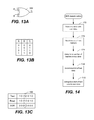
- FIG. 13A shows an XOR gate
- FIG. 13B shows an XOR gate truth table.
- FIG. 13C illustrates XORing of good test data and read test data.
- FIG. 14 illustrates an example of BER determination using test data.
- FIG. 15 shows an example of how BER data may be used.
- FIG. 16 shows how BER data may be used when performing copy operations.
- FIG. 17 shows how BER data may be used when performing read operations.
- FIG. 18 shows how BER data may be used when performing refresh or scrub operations.
- FIG. 19 shows an example of memory system hardware.
- Semiconductor memory devices include volatile memory devices, such as dynamic random access memory (“DRAM”) or static random access memory (“SRAM”) devices, non-volatile memory devices, such as resistive random access memory (“ReRAM”), electrically erasable programmable read only memory (“EEPROM”), flash memory (which can also be considered a subset of EEPROM), ferroelectric random access memory (“FRAM”), and magnetoresistive random access memory (“MRAM”), and other semiconductor elements capable of storing information.
- volatile memory devices such as dynamic random access memory (“DRAM”) or static random access memory (“SRAM”) devices
- non-volatile memory devices such as resistive random access memory (“ReRAM”), electrically erasable programmable read only memory (“EEPROM”), flash memory (which can also be considered a subset of EEPROM), ferroelectric random access memory (“FRAM”), and magnetoresistive random access memory (“MRAM”), and other semiconductor elements capable of storing information.
- ReRAM resistive random access memory
- EEPROM electrically erasable
- the memory devices can be formed from passive and/or active elements, in any combinations.
- passive semiconductor memory elements include ReRAM device elements, which in some embodiments include a resistivity switching storage element, such as an anti-fuse, phase change material, etc., and optionally a steering element, such as a diode, etc.
- active semiconductor memory elements include EEPROM and flash memory device elements, which in some embodiments include elements containing a charge storage region, such as a floating gate, conductive nanoparticles, or a charge storage dielectric material.
- Multiple memory elements may be configured so that they are connected in series or so that each element is individually accessible.
- flash memory devices in a NAND configuration typically contain memory elements connected in series.
- a NAND memory array may be configured so that the array is composed of multiple strings of memory in which a string is composed of multiple memory elements sharing a single bit line and accessed as a group.
- memory elements may be configured so that each element is individually accessible, e.g., a NOR memory array.
- NAND and NOR memory configurations are exemplary, and memory elements may be otherwise configured.
- the semiconductor memory elements located within and/or over a substrate may be arranged in two or three dimensions, such as a two dimensional memory structure or a three dimensional memory structure.
- the semiconductor memory elements are arranged in a single plane or a single memory device level.
- memory elements are arranged in a plane (e.g., in an x-z direction plane) which extends substantially parallel to a major surface of a substrate that supports the memory elements.
- the substrate may be a wafer over or in which the layer of the memory elements are formed or it may be a carrier substrate which is attached to the memory elements after they are formed.
- the substrate may include a semiconductor such as silicon.
- the memory elements may be arranged in the single memory device level in an ordered array, such as in a plurality of rows and/or columns. However, the memory elements may be arrayed in non-regular or non-orthogonal configurations.
- the memory elements may each have two or more electrodes or contact lines, such as bit lines and word lines.
- a three dimensional memory array is arranged so that memory elements occupy multiple planes or multiple memory device levels, thereby forming a structure in three dimensions (i.e., in the x, y and z directions, where the y direction is substantially perpendicular and the x and z directions are substantially parallel to the major surface of the substrate).
- a three dimensional memory structure may be vertically arranged as a stack of multiple two dimensional memory device levels.
- a three dimensional memory array may be arranged as multiple vertical columns (e.g., columns extending substantially perpendicular to the major surface of the substrate, i.e., in the y direction) with each column having multiple memory elements in each column.
- the columns may be arranged in a two dimensional configuration, e.g., in an x-z plane, resulting in a three dimensional arrangement of memory elements with elements on multiple vertically stacked memory planes.
- Other configurations of memory elements in three dimensions can also constitute a three dimensional memory array.
- the memory elements may be coupled together to form a NAND string within a single horizontal (e.g., x-z) memory device levels.
- the memory elements may be coupled together to form a vertical NAND string that traverses across multiple horizontal memory device levels.
- Other three dimensional configurations can be envisioned wherein some NAND strings contain memory elements in a single memory level while other strings contain memory elements which span through multiple memory levels.
- Three dimensional memory arrays may also be designed in a NOR configuration and in a ReRAM configuration.
- a monolithic three dimensional memory array typically, one or more memory device levels are formed above a single substrate.
- the monolithic three dimensional memory array may also have one or more memory layers at least partially within the single substrate.
- the substrate may include a semiconductor such as silicon.
- the layers constituting each memory device level of the array are typically formed on the layers of the underlying memory device levels of the array.
- layers of adjacent memory device levels of a monolithic three dimensional memory array may be shared or have intervening layers between memory device levels.
- non-monolithic stacked memories can be constructed by forming memory levels on separate substrates and then stacking the memory levels atop each other. The substrates may be thinned or removed from the memory device levels before stacking, but as the memory device levels are initially formed over separate substrates, the resulting memory arrays are not monolithic three dimensional memory arrays. Further, multiple two dimensional memory arrays or three dimensional memory arrays (monolithic or non-monolithic) may be formed on separate chips and then packaged together to form a stacked-chip memory device.
- Associated circuitry is typically required for operation of the memory elements and for communication with the memory elements.
- memory devices may have circuitry used for controlling and driving memory elements to accomplish functions such as programming and reading.
- This associated circuitry may be on the same substrate as the memory elements and/or on a separate substrate.
- a controller for memory read-write operations may be located on a separate controller chip and/or on the same substrate as the memory elements.
- FIG. 1 illustrates schematically the main hardware components of a memory system suitable for implementing the present invention.
- the memory system 90 typically operates with a host 80 through a host interface.
- the memory system may be in the form of a removable memory such as a memory card, or may be in the form of an embedded memory system.
- the memory system 90 includes a memory 102 whose operations are controlled by a controller 100 .
- the memory 102 comprises one or more array of non-volatile memory cells distributed over one or more integrated circuit chip.
- the controller 100 may include interface circuits 110 , a processor 120 , ROM (read-only-memory) 122 , RAM (random access memory) 130 , programmable nonvolatile memory 124 , and additional components.
- the controller is typically formed as an ASIC (application specific integrated circuit) and the components included in such an ASIC generally depend on the particular application.
- ASIC application specific integrated circuit
- FIG. 2 illustrates schematically a non-volatile charge storage memory cell.
- the memory cell 10 can be implemented by a field-effect transistor having a charge storage unit 20 , such as a floating gate or a charge trapping (dielectric) layer.
- the memory cell 10 also includes a source 14 , a drain 16 , and a control gate 30 .
- non-volatile solid-state memory devices There are many commercially successful non-volatile solid-state memory devices being used today. These memory devices may employ different types of memory cells, each type having one or more charge storage element.
- Typical non-volatile memory cells include EEPROM and flash EEPROM. Examples of EEPROM cells and methods of manufacturing them are given in U.S. Pat. No. 5,595,924. Examples of flash EEPROM cells, their uses in memory systems and methods of manufacturing them are given in U.S. Pat. Nos. 5,070,032, 5,095,344, 5,315,541, 5,343,063, 5,661,053, 5,313,421 and 6,222,762. In particular, examples of memory devices with NAND cell structures are described in U.S. Pat. Nos. 5,570,315, 5,903,495, 6,046,935.
- the memory state of a cell is usually read by sensing the conduction current across the source and drain electrodes of the cell when a reference voltage is applied to the control gate.
- a corresponding conduction current with respect to a fixed reference control gate voltage may be detected.
- the range of charge programmable onto the floating gate defines a corresponding threshold voltage window or a corresponding conduction current window.
- the threshold voltage for a given memory state under test at the control gate and detect if the conduction current is lower or higher than a threshold current (cell-read reference current).
- the detection of the conduction current relative to a threshold current is accomplished by examining the rate the conduction current is discharging through the capacitance of the bit line.
- FIG. 3 illustrates the relation between the source-drain current I D and the control gate voltage V CG for four different charges Q 1 -Q 4 that the floating gate may be selectively storing at any one time.
- the four solid I D versus V CG curves represent four of seven possible charge levels that can be programmed on a floating gate of a memory cell, respectively corresponding to four possible memory states.
- the threshold voltage window of a population of cells may range from 0.5V to 3.5V. Seven possible programmed memory states “0”, “1”, “2”, “3”, “4”, “5”, “6”, and an erased state (not shown) may be demarcated by partitioning the threshold window into regions in intervals of 0.5V each.
- Q 4 is in a memory state “5”.
- a memory device may have memory cells having a threshold voltage window that ranges from ⁇ 1.5V to 5V. This provides a maximum width of 6.5V. If the memory cell is to store 16 states, each state may occupy from 200 mV to 300 mV in the threshold window. This will require higher precision in programming and reading operations in order to be able to achieve the required resolution.
- FIG. 4A illustrates schematically a string of memory cells organized into a NAND string.
- a pair of select transistors S 1 , S 2 controls the memory transistor chain's connection to the external world via the NAND string's source terminal 54 and drain terminal 56 respectively.
- the source select transistor S 1 when the source select transistor S 1 is turned on, the source terminal is coupled to a source line (see FIG. 4B ).
- the drain select transistor S 2 is turned on, the drain terminal of the NAND string is coupled to a bit line of the memory array.
- Each memory transistor 10 in the chain acts as a memory cell. It has a charge storage element 20 to store a given amount of charge so as to represent an intended memory state.
- a control gate 30 of each memory transistor allows control over read and write operations. As will be seen in FIG. 4B , the control gates 30 of corresponding memory transistors of a row of NAND string are all connected to the same word line. Similarly, a control gate 32 of each of the select transistors S 1 , S 2 provides control access to the NAND string via its source terminal 54 and drain terminal 56 respectively. Likewise, the control gates 32 of corresponding select transistors of a row of NAND string are all connected to the same select line.
- FIG. 4B illustrates an example of a NAND array 210 of memory cells, constituted from NAND strings 50 such as that shown in FIG. 4A .
- a bit line such as bit line 36 is coupled to the drain terminal 56 of each NAND string.
- a source line such as source line 34 is coupled to the source terminals 54 of each NAND string.
- the control gates along a row of memory cells in a bank of NAND strings are connected to a word line such as word line 42 .
- the control gates along a row of select transistors in a bank of NAND strings are connected to a select line such as select line 44 .
- An entire row of memory cells in a bank of NAND strings can be addressed by appropriate voltages on the word lines and select lines of the bank of NAND strings.
- FIG. 5 illustrates a page of memory cells, organized in the NAND configuration, being sensed or programmed in parallel.
- FIG. 5 essentially shows a bank of NAND strings 50 in the memory array 210 of FIG. 4B , where the detail of each NAND string is shown explicitly as in FIG. 4A .
- a physical page such as the page 60 , is a group of memory cells enabled to be sensed or programmed in parallel. This is accomplished by a corresponding page of sense amplifiers 212 . The sensed results are latched in a corresponding set of latches 214 .
- Each sense amplifier can be coupled to a NAND string via a bit line.
- the page is enabled by the control gates of the cells of the page connected in common to a word line 42 and each cell accessible by a sense amplifier accessible via a bit line 36 .
- a sensing voltage or a programming voltage is respectively applied to the common word line WL 3 together with appropriate voltages on the bit lines.
- flash memory One important difference between flash memory and other of types of memory is that a cell must be programmed from the erased state. That is the floating gate must first be emptied of charge. Programming then adds a desired amount of charge back to the floating gate. It does not support removing a portion of the charge from the floating gate to go from a more programmed state to a lesser one. This means that updated data cannot overwrite existing data and must be written to a previous unwritten location.
- the array of memory cells is divided into a large number of blocks of memory cells.
- the block is the unit of erase. That is, each block contains the minimum number of memory cells that are erased together. While aggregating a large number of cells in a block to be erased in parallel will improve erase performance, a large size block also entails dealing with a larger number of update and obsolete data.
- Each block is typically divided into a number of physical pages.
- a logical page is a unit of programming or reading that contains a number of bits equal to the number of cells in a physical page.
- one physical page stores one logical page of data.
- a physical page stores two logical pages. The number of logical pages stored in a physical page thus reflects the number of bits stored per cell.
- the individual pages may be divided into segments and the segments may contain the fewest number of cells that are written at one time as a basic programming operation.
- One or more logical pages of data are typically stored in one row of memory cells.
- a page can store one or more sectors.
- a sector includes user data and overhead data.
- FIG. 6A-6C illustrate an example of programming a population of 4-state memory cells.
- FIG. 6A illustrates the population of memory cells programmable into four distinct distributions of threshold voltages respectively representing memory states “E”, “A”, “B” and “C”. (The vertical axis represents the number of memory cells.)
- FIG. 6B illustrates the initial distribution of “erased” threshold voltages for an erased memory.
- FIG. 6C illustrates an example of the memory after many of the memory cells have been programmed. Essentially, a cell initially has an “erased” threshold voltage and programming will move it to a higher value into one of the three zones demarcated by verify levels vV 1 , vV 2 and vV 3 .
- each memory cell can be programmed to one of the three programmed states “A”, “B” and “C” or remain unprogrammed in the “erased” state.
- the initial distribution of the “erased” state as shown in FIG. 6B will become narrower and the erased state is represented by the “E” state.
- a 2-bit code having a lower bit and an upper bit can be used to represent each of the four memory states.
- the “E”, “A”, “B” and “C” states are respectively represented by “11”, “01”, “00” and ‘10”.
- the 2-bit data may be read from the memory by sensing in “full-sequence” mode where the two bits are sensed together by sensing relative to the read demarcation threshold values rV 1 , rV 2 and rV 3 in three sub-passes respectively.
- An alternative arrangement to a conventional two-dimensional (2-D) NAND array is a three-dimensional (3-D) array.
- 3-D arrays extend up from the wafer surface and generally include stacks, or columns, of memory cells extending upwards.
- Various 3-D arrangements are possible.
- a NAND string is formed vertically with one end (e.g. source) at the wafer surface and the other end (e.g. drain) on top.
- a NAND string is formed in a U-shape so that both ends of the NAND string are accessible on top, thus facilitating connections between such strings. Examples of such NAND strings and their formation are described in U.S. Patent Publication Number 2012/0220088 and in U.S. Patent Publication Number 2013/0107628, which are hereby incorporated by reference in their entirety.
- FIG. 7 shows a first example of a NAND string 701 that extends in a vertical direction, i.e. extending in the z-direction, perpendicular to the x-y plane of the substrate.
- Memory cells are formed where a vertical bit line (local bit line) 703 passes through a word line (e.g. WL 0 , WL 1 , etc.).
- a charge trapping layer between the local bit line and the word line stores charge, which affects the threshold voltage of the transistor formed by the word line (gate) coupled to the vertical bit line (channel) that it encircles.
- Such memory cells may be formed by forming stacks of word lines and then etching memory holes where memory cells are to be formed. Memory holes are then lined with a charge trapping layer and filled with a suitable local bit line/channel material (with suitable dielectric layers for isolation).
- select gates 705 , 707 are located at either end of the string to allow the NAND string to be selectively connected to, or isolated from, external elements 709 , 711 .
- external elements are generally conductive lines such as common source lines or bit lines that serve large numbers of NAND strings.
- Vertical NAND strings may be operated in a similar manner to planar NAND strings and both SLC and MLC operation is possible. While FIG. 7 shows an example of a NAND string that has 32 cells ( 0 - 31 ) connected in series, the number of cells in a NAND string may be any suitable number. Not all cells are shown for clarity. It will be understood that additional cells are formed where word lines 3 - 29 (not shown) intersect the local vertical bit line.
- FIG. 8 shows a second example of a NAND string 815 that extends in a vertical direction (z-direction).
- NAND string 815 forms a U-shape, connecting with external elements (source line “SL” and bit line “BL”) located on the top of the structure.
- source line “SL” and bit line “BL” located on the top of the structure.
- BG controllable gate
- a total of 64 cells are formed where word lines WL 0 -WL 63 intersect the vertical local bit line 817 (though in other examples other numbers of cells may be provided).
- Select gates SGS, SOD are located at either end of NAND string 815 to control connection/isolation of NAND string 815 .
- FIG. 9 shows an example of a three dimensional memory (ReRAM) in which memory elements are formed by resistive elements.
- Global bit lines (GBL 1 -GBL 3 ) extend horizontally in the substrate with select transistors connecting global bit lines to local bit lines (LBL 11 -LBL 33 ).
- Memory cells are formed in horizontal planes that extend above the substrate.
- Word lines in each plane connect to resistive elements of the plane with the opposite ends of the resistive elements connected to local bit lines.
- Word lines extend in pairs in this example (e.g. WL 11 and WL 12 ). In other examples word lines connect to resistive elements on either side and are not paired. Examples of three dimensional ReRAM memory systems are described in U.S. Patent Publication Number 20130229846 by Chien et al.
- data is stored in memory cells by placing memory cells in conditions that are mapped to logical states.
- threshold voltage of a charge storage memory cell such as a floating gate transistor may be mapped into two or more ranges that correspond to different logical states.
- Electrical resistance of a resistive element may be similarly mapped to two or more ranges that correspond to different logic states.
- memory cells retain their programmed condition for an extended period of time without further intervention. However, some change generally occurs over time for a variety of reasons so that data may not be read exactly as it was programmed.
- Some bits may be flipped (i.e. some cells that were programmed with a logic 0 are read as logic 1 and some cells programmed with a logic 1 are read as logic 0).
- the number of such flipped bits (bad bits) in a given portion of data may be expressed as the Bit Error Rate (“BER”) which may be expressed as a fraction, ratio, percentage, or other suitable format.
- BER Bit Error Rate
- the BER gives an indication of the condition or health of the data, which may be used in various ways.
- Data that is read from a memory may be handled differently depending on the BER of the data. For example, different approaches to correcting the data may be used depending on the BER.
- Data with a low BER may be corrected by a simple ECC decoding scheme prior to being sent to a host (or may be copied to another location within the memory without any correction).
- Data with a higher BER may require a different ECC correction scheme.
- Data with a high BER may be uncorrectable by ECC and may require some other form of correction or recovery.
- ECC decoding may take significant time and resources to determine BER for a portion of data and ECC correction is generally performed in a controller or other IC that is separate from the memory IC so that data transfer is required. Aspects of the present invention are directed to fast and efficient ways to obtain an indication of BER which may then be used to make decisions as to how the data should be handled (including whether ECC decoding should be applied, and if so what sort of ECC decoding).
- FIGS. 10A-10C illustrate data that is programmed and subsequently read from a charge storage SLC memory.
- FIG. 10A shows a population of memory cells that are in the erased state prior to programming.
- FIG. 10A shows threshold voltage V TH along the horizontal axis and the number of cells along the vertical axis.
- FIG. 10B the memory cells are programmed so that threshold voltages of some memory cells are increased to a range that corresponds to a logic state 0 while threshold voltages of other memory cells remain substantially unchanged in a range that corresponds to a logic state 1 (mapping of logic states to threshold voltage ranges may also be the opposite with logic 1 corresponding to programmed cells and logic 0 corresponding to unprogrammed cells).
- threshold voltages of memory cells may change because of charge leakage, disturbance from other memory access operations (e.g. because of programming of other data, or reading operations), physical defects, or other reasons. These distributions may cause some bad bits when the data is read. For example, the distribution of memory cells programmed to logic 0 extends below the read voltage rV so that these cells are misread as logic 1. Similarly, the distribution of memory cells programmed to logic 1 extends above rV so that these cells are misread as logic 0.
- FIGS. 10D-10E illustrate bit flipping more generally for two-state memories (including resistive memories, or memories using other physical characteristics to store data). After data is programmed, some cells flip from logic 0 to logic 1 and some flip from logic 1 to logic 0. This may result in a change in the overall distribution or shape of the memory cells as shown by FIG. 10E . While FIG. 10D shows more logic 1 cells than logic 0 cells, FIG. 10E shows more logic 0 cells than logic 1 cells. According to an example, a change in overall distribution or shape may be detected and used to provide an indication of BER. An indication of the shape may be recorded at the time of writing the data in the memory. Subsequently, when the data is read, the shape of the read data is again determined and is compared with the recorded shape.
- the initial shape might be recorded as a number, a fraction, or percentage of cells in the logic 1 state (e.g. 700, 0.7, or 70% for a population of 1000 cells) while the shape of the read data would be a different number, fraction, or percentage (e.g. 400, 0.4, or 40%).
- a different number, fraction, or percentage e.g. 400, 0.4, or 40%.
- the profile or shape of a population of programmed memory cells in an MLC memory may be similarly identified and recorded.
- the fraction of memory cells in each state, or a subset of the four states may be recorded for subsequent comparison with corresponding fractions in read data.
- Estimation of BER from shape information may be performed in any suitable manner depending on the nature of the data and the memory cells. Some data may not have a normal distribution of logic states but instead may be have an asymmetric distribution that is skewed towards particular logic states. This may occur randomly or because of a deliberate shaping operation that is implemented to achieve a particular shape to improve memory operation. For example, data in ReRAM may be shaped to favor higher resistance states. In some memories, memory cells may flip symmetrically (i.e. equal numbers of cells flip from 0 to 1 and from 1 to 0) while in other memories memory cells may flip asymmetrically. Such characteristics may be factored in when calculating BER.
- FIG. 11 illustrates a scheme for determining BER from shape information.
- An indicator of data shape is recorded 150 when the data is written. Subsequently, when the data is read from the memory 152 , the shape of the read data is determined 154 . The difference between the shape of the written data and the shape of the read data may then be used to determine the BER 156 .
- Shape data may be obtained in a fairly simple manner. For example, data that is held in a row of latches may be subject to a bit scan operation in which the number of latches in a particular state (e.g. logic 1) are counted. This can be done prior to programming a portion of data and the result can be stored. When the data is read another bit scan is performed to count the number of cells in the particular state. Any change can be used to determine the BER of the data.
- a particular state e.g. logic 1
- BER estimation from changes in data shape may not be suitable for all situations. For example, if data is not shaped prior to storage and is more randomized (e.g. SLC memory cells approximately 50% zeroes) and flipping is symmetric, then the number of bits flipped in each direction will be equal so that the shape of the data remains the same regardless of the number of bits flipped.
- randomized e.g. SLC memory cells approximately 50% zeroes
- certain stored data may be read and compared with a good copy of the data to determine the number of bad bits and thus the BER.
- This approach may be suitable for some cases where BER estimation from data shape is not suitable, for example, where bits are flipped in a substantially symmetric manner (the number of bits flipped from one to zero is approximately equal to the number of bits flipped from zero to one) so that bad bits do not affect overall data shape.
- the data may be a portion of test data that has a predetermined pattern that is easily reproduced so that a good copy can be generated whenever it is needed, for example all ones, all zeroes, alternating ones and zeroes, or some other simple pattern.
- FIG. 12 shows an example of test data in the top row.
- the test data consists of alternating ones and zeroes which can be easily generated.
- This test data may be stored in a memory and later read.
- a portion of a memory may be considered as a test area that is not used for storage of user data but instead is used for test data.
- Such a test area may be included in each plane, in each block, or in some other arrangement, and may be static or may be relocated as desired.
- the test data is read from the memory as shown by the lower row. This may occur after the data has been stored for a significant period of time.
- the read copy is compared to a good copy to identify any flipped bits. In FIG. 12 , one bit 160 flipped from zero to one. By counting all such bits in a portion of test data the BER may be obtained for the test data.
- FIG. 13A shows an XOR gate 164 that may be implemented in any suitable manner.
- FIG. 13B is a truth table for the XOR gate 164 of FIG. 13A showing that the output (C) is zero when the inputs (A and B) are the same. The output is one only when inputs are different.
- FIG. 13C illustrates comparison by XORing of good test data (top row), read data (middle row), to provide an XOR output (bottom row) in which a one represents a flipped bit 168 .
- FIG. 14 illustrates how BER may be determined using test data.
- the test data is stored with user data 170 . This may be done so that the test data experiences the same conditions as the user data.
- the test data may be stored at the same time as the user data, or shortly after, and may be stored at the same physical location, or a close physical location.
- the cells used to store such test data may be referred to as “reference cells” used for reference to estimate the BER of associated user data.
- the test data may be in reference cells in the same page, block, or plane as the user data.
- test data may be written in relatively small chunks that are smaller than units of writing of user data.
- some ReRAM memories allow writing of relatively small portions of data that are smaller than a conventional page in flash memory.
- test data may be written separately or in parallel with writing of user data and may subsequently be read separately or in parallel with user data.
- a portion of test data may be written whenever a new host write command is received so and that test data is then used to estimate the BER for data stored in response to the write command.
- test data may be written in a block when writing of user data starts in the block. The test data may then be used to estimate the BER of data stored in the block. Subsequently, the test data is read from the memory 172 . This may occur when user data is to be read (e.g. in response to a host read command) or as part of an internal memory operation (e.g.
- the read test data is compared with a good copy of the data to determine the number of bad bits in the test data 174 .
- the number of bad bits gives the BER of the test data.
- the BER of the test data is then extrapolated to user data 178 .
- a BER estimate such as obtained from one of the techniques described above may be used to indicate the health of stored data and has several practical applications in memory operations. In general, knowing the BER of a particular portion of data allows that data to be handled in a manner that is appropriate. Data with a high BER may be handled differently to data with a low BER.
- FIG. 15 illustrates how BER estimation may be applied to data handling.
- Data to be handled is first identified 500 .
- a read command from a host may identify such data.
- data may be identified by a memory controller as being due for some housekeeping operation such as garbage collection or scrubbing.
- the BER of the identified data is then estimated 502 , for example by comparing the shape of the identified data prior to storage and after storage, or by comparing stored test data with a good copy of the test data, or otherwise.
- An appropriate manner of handling the data is then selected based on the BER of the data 504 .
- the BER is stored so that the health is tracked over time in a table or other form.
- This allows mapping of data health across a memory (e.g. page-by-page, block-by-block, die-by-die, or in some other unit) over time. This may provide some information on the rate of decay of stored data which may give a rough estimate of how long the data may be expected to remain good. It may also help to identify blocks that are close to becoming bad blocks before they become unusable (thus avoiding any loss of user data).
- Periodic health checks may be performed on portions of the memory so that data health information remains up to date. This data may be used to determine how to prioritize refresh or scrub operations and how data should be read, copied, and decoded.
- FIG. 16 illustrates an example of how BER information may be used when copying data from one location in a memory to another as part of an internal copy operation. For example, such data may be copied to a new location during garbage collection or consolidation of valid data.
- the BER of the data to be copied is determined 610 . If the BER is not below a threshold 612 then the data may be sent off-chip (e.g. to a memory controller) for ECC correction 614 . The corrected data may be sent back to the memory for storage. If the BER is below the threshold 612 then the data may be copied to another location on the same memory chip without ECC correction 616 . This provides a simple fast manner of copying data without using resources of the memory controller or using the memory bus between the memory and controller.
- the threshold above which ECC correction is required depends on the ECC correction capacity available. It is generally desirable to perform ECC correction if there is a significant probability that the data, if copied without correction, would become uncorrectable by ECC (UECC) by the next time it is read. Thus, for example, where an ECC scheme can correct 10 bad bits per page, it may be considered acceptable to copy a page that contains 3 bad bits without ECC correction while it may be considered unacceptable to copy a page that contains 7 bad bits without ECC correction because such data is closer to becoming UECC.
- FIG. 17 illustrates an example of how BER information may be used when reading data from a memory.
- the BER of data to be read is determined 720 .
- a determination is made as to whether the BER is below a threshold 722 . If the BER is below the threshold then the data may be sent to a memory controller 724 where the data may be subject to ECC decoding (and may be sent on to a host after decoding). If the BER is not below the threshold 722 then the data may be reread using modified read parameters 726 . For example, a different read voltage may be applied and/or different read pass voltages may be applied, or a higher resolution read operation may be used. The BER of the reread data is determined and compared with the threshold.
- This cycle may be repeated with different read conditions until data is read with a BER that is below the threshold. If suitable read conditions are found they may be recorded for subsequent read operations in the block or other unit. The operation may terminate if some maximum time, or maximum number of cycles, is reached without obtaining acceptable data.
- an appropriate error correction scheme may be chosen according to the BER in the read data. For example, different ECC decoding approaches may be used depending on the BER estimated. Certain ECC engines support multiple decoding modes. In some cases, a simple fast mode may be applied if the BER is low and a more complex slower mode may be applied if the BER is higher. For example, an indication of a high BER may result in selection of an advanced ECC decoding mode, which may use more power and/or require more time. This may allow appropriate ECC decoding of data with different BERs so that relatively good data is decoded rapidly and efficiently, and more advanced ECC decoding is used sparingly for relatively bad (noisy but still correctable) data.
- Two or more ECC decoding modes or schemes may be applied to data according to estimated BER so that ECC decoding is tailored to the quality of a particular portion of data to be decoded. If the BER indicates that the data is UECC then ECC correction may be skipped in favor of recovering the data in some other manner, or some other approach may be used first to obtain correctable data which is then sent for ECC decoding. For example, a modified read scheme may be used to obtain correctable data which is then sent for ECC correction. This saves the significant resources that may be consumed attempting to correct UECC data. For example, Low Density Parity Check (LDPC) decoding may take significant time and resources.
- LDPC Low Density Parity Check
- FIG. 18 illustrates an example of how BER information may be used when performing a refresh or scrub operation in a memory.
- a refresh operation rewrites data into the same cells to improve the quality of the data while a scrub operation rewrites the data to another location in memory and makes the old copy obsolete thus allowing it to be erased.
- Certain ReRAM memories may be refreshed while many charge storage memories are scrubbed.
- the BER of the data may be determined 830 . The BER is then compared with a threshold 832 . If the BER is below the threshold then the operation may proceed to the next data 834 without performing refresh or scrub. Thus, if the BER indicates that the data is in good condition (e.g.
- FIG. 19 illustrates an example of hardware that may be used to implement some of the techniques described above.
- a memory system 400 includes a memory controller 402 and a memory integrated circuit (IC) 404 connected by a memory bus. Additional memory ICs may also be connected to the memory controller by the bus and/or by additional busses.
- the memory IC 404 includes a memory array 406 , which may be a two dimensional (planar) memory array or a three dimensional memory array with multiple physical levels disposed above a substrate.
- the memory may store two bits per cell (SLC) or may store more than two bits per cell (MLC) and may use charge storage, electrical resistance, or other physical property.
- the memory IC includes peripheral circuits 408 including BER calculation circuits 410 that may include circuits that record the shapes of data prior to storage and after storage and calculate BER from the difference between these shapes. These circuits may include bit scan circuits that count the number of bits of a particular logic state (e.g. logic 0). BER calculation circuits 410 may include XOR circuits that compare test data read from the memory array with a good copy of test data to determine the number of bad bits. Copy circuits 412 in the memory IC 404 allow on-chip copy to be performed (i.e. allow copying of data from one location in the memory array to another location in the memory array without sending the data outside the memory IC 404 ).
- Copy circuits may include one or more rows of data latches that can receive data from the memory, hold the data, and then transfer the data for programming.
- Memory controller 402 includes ECC circuits 414 such as LDPC circuits for encoding data prior to storage and decoding data after storage. Controller 402 also contains a table 416 that records the health of data in memory array 406 based on BER of the data. The table may record BER, or a metric derived from BER, for each page, block, or some other unit. The table may be updated as appropriate.
Abstract
Description
P zero-at-prog=0.2,P zero-at-read=0.22
The number of zeroes read is the original number of zeroes minus the number of cells that flipped from zero to one, plus the number of cells that have flipped from one to zero. Assuming that the probability of flipping (“Prob”) is symmetric, this may be expressed as:
P zero-at-read =P zero-at-prog*(1−Prob)+(1−P zero-at-prod)*Prob
Substituting in the numbers above gives:
0.22=0.2*(1−Prob)+(0.8)*Prob
Solving for Prob gives:
Prob=0.033, or 3.3%
Thus, the change in shape from 20% to 22% zeroes corresponds to a probability of flipping of 3.3% and a BER of 3.3%. This estimation has a standard deviation of approximately:
Sqrt(n*Prob*(1−Prob))/n=0.002, or 0.2% where n is the number of cells.
Claims (31)
Priority Applications (1)
| Application Number | Priority Date | Filing Date | Title |
|---|---|---|---|
| US14/318,310 US9483339B2 (en) | 2014-06-27 | 2014-06-27 | Systems and methods for fast bit error rate estimation |
Applications Claiming Priority (1)
| Application Number | Priority Date | Filing Date | Title |
|---|---|---|---|
| US14/318,310 US9483339B2 (en) | 2014-06-27 | 2014-06-27 | Systems and methods for fast bit error rate estimation |
Publications (2)
| Publication Number | Publication Date |
|---|---|
| US20150378801A1 US20150378801A1 (en) | 2015-12-31 |
| US9483339B2 true US9483339B2 (en) | 2016-11-01 |
Family
ID=54930602
Family Applications (1)
| Application Number | Title | Priority Date | Filing Date |
|---|---|---|---|
| US14/318,310 Active 2034-10-22 US9483339B2 (en) | 2014-06-27 | 2014-06-27 | Systems and methods for fast bit error rate estimation |
Country Status (1)
| Country | Link |
|---|---|
| US (1) | US9483339B2 (en) |
Families Citing this family (17)
| Publication number | Priority date | Publication date | Assignee | Title |
|---|---|---|---|---|
| US9965345B2 (en) * | 2014-09-24 | 2018-05-08 | Macronix International Co., Ltd. | Health management of non-volatile memory |
| US9773563B2 (en) * | 2015-03-27 | 2017-09-26 | Toshiba Memory Corporation | Memory controller, memory control method, and coefficient decision method |
| US9780809B2 (en) * | 2015-04-30 | 2017-10-03 | Sandisk Technologies Llc | Tracking and use of tracked bit values for encoding and decoding data in unreliable memory |
| US9823987B1 (en) * | 2015-10-02 | 2017-11-21 | Seagate Technology Llc | Data quality pre-selection in read retry operations |
| US10579290B2 (en) * | 2016-03-23 | 2020-03-03 | Winbond Electronics Corp. | Option code providing circuit and providing method thereof |
| CN106027172B (en) * | 2016-04-22 | 2021-05-04 | 北京联盛德微电子有限责任公司 | Method and device for testing receiver chip |
| US10983865B2 (en) * | 2016-08-01 | 2021-04-20 | Hewlett Packard Enterprise Development Lp | Adjusting memory parameters |
| US10657014B2 (en) * | 2017-02-27 | 2020-05-19 | Everspin Technologies, Inc. | Methods for monitoring and managing memory devices |
| US10318381B2 (en) * | 2017-03-29 | 2019-06-11 | Micron Technology, Inc. | Selective error rate information for multidimensional memory |
| US10445190B2 (en) * | 2017-11-08 | 2019-10-15 | Alibaba Group Holding Limited | Method and system for enhancing backup efficiency by bypassing encoding and decoding |
| US10698610B2 (en) * | 2018-02-23 | 2020-06-30 | Western Digital Technologies, Inc. | Storage system and method for performing high-speed read and write operations |
| KR102483476B1 (en) * | 2018-04-03 | 2023-01-03 | 에스케이하이닉스 주식회사 | Semiconductor memory apparatus supporting repair with data I/O terminal as a unit and method of repairing the semiconductor memory apparatus |
| CN110751974A (en) * | 2018-07-23 | 2020-02-04 | 爱思开海力士有限公司 | Memory system and method for optimizing read threshold |
| US10643719B2 (en) * | 2018-09-04 | 2020-05-05 | Micron Technology, Inc. | Enhanced read disturbance detection and remediation for a memory sub-system |
| US11216349B2 (en) * | 2018-10-12 | 2022-01-04 | Micron Technology, Inc. | Reactive read based on metrics to screen defect prone memory blocks |
| US11500719B1 (en) * | 2020-03-31 | 2022-11-15 | Amazon Technologies, Inc. | Reliability improvements for memory technologies |
| US11797385B2 (en) * | 2021-10-25 | 2023-10-24 | Micron Technology, Inc. | Managing information protection schemes in memory systems |
Citations (18)
| Publication number | Priority date | Publication date | Assignee | Title |
|---|---|---|---|---|
| US5070032A (en) | 1989-03-15 | 1991-12-03 | Sundisk Corporation | Method of making dense flash eeprom semiconductor memory structures |
| US5095344A (en) | 1988-06-08 | 1992-03-10 | Eliyahou Harari | Highly compact eprom and flash eeprom devices |
| US5313421A (en) | 1992-01-14 | 1994-05-17 | Sundisk Corporation | EEPROM with split gate source side injection |
| US5315541A (en) | 1992-07-24 | 1994-05-24 | Sundisk Corporation | Segmented column memory array |
| US5343063A (en) | 1990-12-18 | 1994-08-30 | Sundisk Corporation | Dense vertical programmable read only memory cell structure and processes for making them |
| US5570315A (en) | 1993-09-21 | 1996-10-29 | Kabushiki Kaisha Toshiba | Multi-state EEPROM having write-verify control circuit |
| US5595924A (en) | 1994-05-25 | 1997-01-21 | Sandisk Corporation | Technique of forming over an irregular surface a polysilicon layer with a smooth surface |
| US5768192A (en) | 1996-07-23 | 1998-06-16 | Saifun Semiconductors, Ltd. | Non-volatile semiconductor memory cell utilizing asymmetrical charge trapping |
| US5903495A (en) | 1996-03-18 | 1999-05-11 | Kabushiki Kaisha Toshiba | Semiconductor device and memory system |
| US6011725A (en) | 1997-08-01 | 2000-01-04 | Saifun Semiconductors, Ltd. | Two bit non-volatile electrically erasable and programmable semiconductor memory cell utilizing asymmetrical charge trapping |
| US6222762B1 (en) | 1992-01-14 | 2001-04-24 | Sandisk Corporation | Multi-state memory |
| US20130107628A1 (en) | 2011-11-02 | 2013-05-02 | Yingda Dong | Selective Word Line Erase In 3D Non-Volatile Memory |
| US20130220088A1 (en) | 2009-07-31 | 2013-08-29 | Groz-Beckert Kg | Punch Tool With a Stamp Supported in a Floating Manner |
| US20130229846A1 (en) | 2010-12-14 | 2013-09-05 | Sandisk 3D Llc | Memories with Cylindrical Read/Write Stacks |
| US20140043897A1 (en) | 2012-08-07 | 2014-02-13 | Feng Pan | Aggregating data latches for program level determination |
| US20140043898A1 (en) | 2012-08-07 | 2014-02-13 | Tien-chien Kuo | Common Line Current for Program Level Determination in Flash Memory |
| US20150121157A1 (en) * | 2013-10-28 | 2015-04-30 | Sandisk Technologies Inc. | Selection of Data for Redundancy Calculation By Likely Error Rate |
| US20150348649A1 (en) * | 2014-06-03 | 2015-12-03 | Sandisk Technologies Inc. | Bit error rate mapping in a memory system |
-
2014
- 2014-06-27 US US14/318,310 patent/US9483339B2/en active Active
Patent Citations (20)
| Publication number | Priority date | Publication date | Assignee | Title |
|---|---|---|---|---|
| US5095344A (en) | 1988-06-08 | 1992-03-10 | Eliyahou Harari | Highly compact eprom and flash eeprom devices |
| US5070032A (en) | 1989-03-15 | 1991-12-03 | Sundisk Corporation | Method of making dense flash eeprom semiconductor memory structures |
| US5343063A (en) | 1990-12-18 | 1994-08-30 | Sundisk Corporation | Dense vertical programmable read only memory cell structure and processes for making them |
| US6222762B1 (en) | 1992-01-14 | 2001-04-24 | Sandisk Corporation | Multi-state memory |
| US5313421A (en) | 1992-01-14 | 1994-05-17 | Sundisk Corporation | EEPROM with split gate source side injection |
| US5315541A (en) | 1992-07-24 | 1994-05-24 | Sundisk Corporation | Segmented column memory array |
| US5570315A (en) | 1993-09-21 | 1996-10-29 | Kabushiki Kaisha Toshiba | Multi-state EEPROM having write-verify control circuit |
| US5595924A (en) | 1994-05-25 | 1997-01-21 | Sandisk Corporation | Technique of forming over an irregular surface a polysilicon layer with a smooth surface |
| US5661053A (en) | 1994-05-25 | 1997-08-26 | Sandisk Corporation | Method of making dense flash EEPROM cell array and peripheral supporting circuits formed in deposited field oxide with the use of spacers |
| US5903495A (en) | 1996-03-18 | 1999-05-11 | Kabushiki Kaisha Toshiba | Semiconductor device and memory system |
| US6046935A (en) | 1996-03-18 | 2000-04-04 | Kabushiki Kaisha Toshiba | Semiconductor device and memory system |
| US5768192A (en) | 1996-07-23 | 1998-06-16 | Saifun Semiconductors, Ltd. | Non-volatile semiconductor memory cell utilizing asymmetrical charge trapping |
| US6011725A (en) | 1997-08-01 | 2000-01-04 | Saifun Semiconductors, Ltd. | Two bit non-volatile electrically erasable and programmable semiconductor memory cell utilizing asymmetrical charge trapping |
| US20130220088A1 (en) | 2009-07-31 | 2013-08-29 | Groz-Beckert Kg | Punch Tool With a Stamp Supported in a Floating Manner |
| US20130229846A1 (en) | 2010-12-14 | 2013-09-05 | Sandisk 3D Llc | Memories with Cylindrical Read/Write Stacks |
| US20130107628A1 (en) | 2011-11-02 | 2013-05-02 | Yingda Dong | Selective Word Line Erase In 3D Non-Volatile Memory |
| US20140043897A1 (en) | 2012-08-07 | 2014-02-13 | Feng Pan | Aggregating data latches for program level determination |
| US20140043898A1 (en) | 2012-08-07 | 2014-02-13 | Tien-chien Kuo | Common Line Current for Program Level Determination in Flash Memory |
| US20150121157A1 (en) * | 2013-10-28 | 2015-04-30 | Sandisk Technologies Inc. | Selection of Data for Redundancy Calculation By Likely Error Rate |
| US20150348649A1 (en) * | 2014-06-03 | 2015-12-03 | Sandisk Technologies Inc. | Bit error rate mapping in a memory system |
Non-Patent Citations (1)
| Title |
|---|
| Eitan et al., "NROM: A Novel Localized Trapping, 2-Bit Nonvolatile Memory Cell," IEEE Electron Device Letters, vol. 21, No. 11, Nov. 2000, pp. 543-545. |
Also Published As
| Publication number | Publication date |
|---|---|
| US20150378801A1 (en) | 2015-12-31 |
Similar Documents
| Publication | Publication Date | Title |
|---|---|---|
| US9483339B2 (en) | Systems and methods for fast bit error rate estimation | |
| US9015561B1 (en) | Adaptive redundancy in three dimensional memory | |
| US9558847B2 (en) | Defect logging in nonvolatile memory | |
| US8902652B1 (en) | Systems and methods for lower page writes | |
| US9105349B2 (en) | Adaptive operation of three dimensional memory | |
| US8887011B2 (en) | Erased page confirmation in multilevel memory | |
| US8886877B1 (en) | In-situ block folding for nonvolatile memory | |
| US9411669B2 (en) | Selective sampling of data stored in nonvolatile memory | |
| US9092363B2 (en) | Selection of data for redundancy calculation in three dimensional nonvolatile memory | |
| US9792175B2 (en) | Bad column management in nonvolatile memory | |
| CN107112044B (en) | Multi-chip dual write | |
| US9484098B1 (en) | Smart reread in nonvolatile memory | |
| US9659666B2 (en) | Dynamic memory recovery at the sub-block level | |
| US9136022B2 (en) | Selection of data for redundancy calculation by likely error rate | |
| WO2016069126A1 (en) | Read scrub with adaptive read counter management | |
| US9063671B2 (en) | Write operations with full sequence programming for defect management in nonvolatile memory | |
| US8918577B1 (en) | Three dimensional nonvolatile memory with variable block capacity | |
| US9583207B2 (en) | Adaptive data shaping in nonvolatile memory | |
| TW201511024A (en) | Efficient post write read in three dimensional nonvolatile memory | |
| US20160259570A1 (en) | Block Management Scheme to Handle Cluster Failures in Non-Volatile Memory | |
| WO2016057158A1 (en) | Nonvolatile memory and method with state encoding and page-by-page programming yielding invariant read points |
Legal Events
| Date | Code | Title | Description |
|---|---|---|---|
| AS | Assignment |
Owner name: SANDISK TECHNOLOGIES INC., TEXAS Free format text: ASSIGNMENT OF ASSIGNORS INTEREST;ASSIGNORS:NAVON, ARIEL;SHARON, ERAN;REEL/FRAME:033219/0641 Effective date: 20140615 |
|
| AS | Assignment |
Owner name: SANDISK TECHNOLOGIES LLC, TEXAS Free format text: CHANGE OF NAME;ASSIGNOR:SANDISK TECHNOLOGIES INC;REEL/FRAME:038807/0807 Effective date: 20160516 |
|
| STCF | Information on status: patent grant |
Free format text: PATENTED CASE |
|
| MAFP | Maintenance fee payment |
Free format text: PAYMENT OF MAINTENANCE FEE, 4TH YEAR, LARGE ENTITY (ORIGINAL EVENT CODE: M1551); ENTITY STATUS OF PATENT OWNER: LARGE ENTITY Year of fee payment: 4 |