US9552291B2 - Memory management method - Google Patents
Memory management method Download PDFInfo
- Publication number
- US9552291B2 US9552291B2 US14/722,532 US201514722532A US9552291B2 US 9552291 B2 US9552291 B2 US 9552291B2 US 201514722532 A US201514722532 A US 201514722532A US 9552291 B2 US9552291 B2 US 9552291B2
- Authority
- US
- United States
- Prior art keywords
- data
- nvram
- dram
- computer
- page
- Prior art date
- Legal status (The legal status is an assumption and is not a legal conclusion. Google has not performed a legal analysis and makes no representation as to the accuracy of the status listed.)
- Expired - Fee Related
Links
Images


Classifications
-
- G—PHYSICS
- G06—COMPUTING; CALCULATING OR COUNTING
- G06F—ELECTRIC DIGITAL DATA PROCESSING
- G06F12/00—Accessing, addressing or allocating within memory systems or architectures
- G06F12/02—Addressing or allocation; Relocation
- G06F12/0223—User address space allocation, e.g. contiguous or non contiguous base addressing
- G06F12/023—Free address space management
- G06F12/0238—Memory management in non-volatile memory, e.g. resistive RAM or ferroelectric memory
- G06F12/0246—Memory management in non-volatile memory, e.g. resistive RAM or ferroelectric memory in block erasable memory, e.g. flash memory
-
- G—PHYSICS
- G06—COMPUTING; CALCULATING OR COUNTING
- G06F—ELECTRIC DIGITAL DATA PROCESSING
- G06F3/00—Input arrangements for transferring data to be processed into a form capable of being handled by the computer; Output arrangements for transferring data from processing unit to output unit, e.g. interface arrangements
- G06F3/06—Digital input from, or digital output to, record carriers, e.g. RAID, emulated record carriers or networked record carriers
- G06F3/0601—Interfaces specially adapted for storage systems
- G06F3/0628—Interfaces specially adapted for storage systems making use of a particular technique
- G06F3/0629—Configuration or reconfiguration of storage systems
- G06F3/0634—Configuration or reconfiguration of storage systems by changing the state or mode of one or more devices
-
- G—PHYSICS
- G06—COMPUTING; CALCULATING OR COUNTING
- G06F—ELECTRIC DIGITAL DATA PROCESSING
- G06F12/00—Accessing, addressing or allocating within memory systems or architectures
- G06F12/02—Addressing or allocation; Relocation
- G06F12/06—Addressing a physical block of locations, e.g. base addressing, module addressing, memory dedication
- G06F12/0638—Combination of memories, e.g. ROM and RAM such as to permit replacement or supplementing of words in one module by words in another module
-
- G—PHYSICS
- G06—COMPUTING; CALCULATING OR COUNTING
- G06F—ELECTRIC DIGITAL DATA PROCESSING
- G06F3/00—Input arrangements for transferring data to be processed into a form capable of being handled by the computer; Output arrangements for transferring data from processing unit to output unit, e.g. interface arrangements
- G06F3/06—Digital input from, or digital output to, record carriers, e.g. RAID, emulated record carriers or networked record carriers
- G06F3/0601—Interfaces specially adapted for storage systems
- G06F3/0602—Interfaces specially adapted for storage systems specifically adapted to achieve a particular effect
- G06F3/0604—Improving or facilitating administration, e.g. storage management
-
- G—PHYSICS
- G06—COMPUTING; CALCULATING OR COUNTING
- G06F—ELECTRIC DIGITAL DATA PROCESSING
- G06F3/00—Input arrangements for transferring data to be processed into a form capable of being handled by the computer; Output arrangements for transferring data from processing unit to output unit, e.g. interface arrangements
- G06F3/06—Digital input from, or digital output to, record carriers, e.g. RAID, emulated record carriers or networked record carriers
- G06F3/0601—Interfaces specially adapted for storage systems
- G06F3/0628—Interfaces specially adapted for storage systems making use of a particular technique
- G06F3/0646—Horizontal data movement in storage systems, i.e. moving data in between storage devices or systems
- G06F3/0647—Migration mechanisms
-
- G—PHYSICS
- G06—COMPUTING; CALCULATING OR COUNTING
- G06F—ELECTRIC DIGITAL DATA PROCESSING
- G06F3/00—Input arrangements for transferring data to be processed into a form capable of being handled by the computer; Output arrangements for transferring data from processing unit to output unit, e.g. interface arrangements
- G06F3/06—Digital input from, or digital output to, record carriers, e.g. RAID, emulated record carriers or networked record carriers
- G06F3/0601—Interfaces specially adapted for storage systems
- G06F3/0668—Interfaces specially adapted for storage systems adopting a particular infrastructure
- G06F3/0671—In-line storage system
- G06F3/0683—Plurality of storage devices
- G06F3/0685—Hybrid storage combining heterogeneous device types, e.g. hierarchical storage, hybrid arrays
-
- G—PHYSICS
- G06—COMPUTING; CALCULATING OR COUNTING
- G06F—ELECTRIC DIGITAL DATA PROCESSING
- G06F9/00—Arrangements for program control, e.g. control units
- G06F9/06—Arrangements for program control, e.g. control units using stored programs, i.e. using an internal store of processing equipment to receive or retain programs
- G06F9/44—Arrangements for executing specific programs
- G06F9/4401—Bootstrapping
- G06F9/4406—Loading of operating system
-
- G—PHYSICS
- G11—INFORMATION STORAGE
- G11C—STATIC STORES
- G11C11/00—Digital stores characterised by the use of particular electric or magnetic storage elements; Storage elements therefor
- G11C11/21—Digital stores characterised by the use of particular electric or magnetic storage elements; Storage elements therefor using electric elements
- G11C11/34—Digital stores characterised by the use of particular electric or magnetic storage elements; Storage elements therefor using electric elements using semiconductor devices
- G11C11/40—Digital stores characterised by the use of particular electric or magnetic storage elements; Storage elements therefor using electric elements using semiconductor devices using transistors
- G11C11/401—Digital stores characterised by the use of particular electric or magnetic storage elements; Storage elements therefor using electric elements using semiconductor devices using transistors forming cells needing refreshing or charge regeneration, i.e. dynamic cells
- G11C11/4063—Auxiliary circuits, e.g. for addressing, decoding, driving, writing, sensing or timing
- G11C11/407—Auxiliary circuits, e.g. for addressing, decoding, driving, writing, sensing or timing for memory cells of the field-effect type
- G11C11/409—Read-write [R-W] circuits
- G11C11/4096—Input/output [I/O] data management or control circuits, e.g. reading or writing circuits, I/O drivers or bit-line switches
-
- G—PHYSICS
- G06—COMPUTING; CALCULATING OR COUNTING
- G06F—ELECTRIC DIGITAL DATA PROCESSING
- G06F2212/00—Indexing scheme relating to accessing, addressing or allocation within memory systems or architectures
- G06F2212/20—Employing a main memory using a specific memory technology
- G06F2212/205—Hybrid memory, e.g. using both volatile and non-volatile memory
-
- G—PHYSICS
- G06—COMPUTING; CALCULATING OR COUNTING
- G06F—ELECTRIC DIGITAL DATA PROCESSING
- G06F2212/00—Indexing scheme relating to accessing, addressing or allocation within memory systems or architectures
- G06F2212/72—Details relating to flash memory management
- G06F2212/7201—Logical to physical mapping or translation of blocks or pages
-
- G—PHYSICS
- G11—INFORMATION STORAGE
- G11C—STATIC STORES
- G11C14/00—Digital stores characterised by arrangements of cells having volatile and non-volatile storage properties for back-up when the power is down
- G11C14/0009—Digital stores characterised by arrangements of cells having volatile and non-volatile storage properties for back-up when the power is down in which the volatile element is a DRAM cell
Definitions
- the present invention relates to a memory management method, and particularly relates to a method for managing main memory including DRAM and NVRAM in a computer depending on the operation state of the computer.
- Nonvolatile memory hereafter referred to as “NVRAM”) is currently in active research and development.
- NVRAM Nonvolatile memory
- the use of NVRAM is expected to achieve a memory system with higher integration, lower power, and lower cost in the future. This gives rise to the proposal to use DRAM and NVRAM in main storage memory in a computer.
- NVRAM has drawbacks such as longer write times, higher write power consumption, a larger unit of writing, and lower write endurance than DRAM. These drawbacks need to be compensated for in order to use NVRAM as main storage memory, but sufficient improvements for actual use have not been made.
- NVRAM is at best merely utilized for a data backup of main storage memory in actual use.
- the present invention thus has an object of enabling the use of NVRAM as main storage memory in a computer, and particularly an object of providing a method for managing main memory including DRAM and NVRAM in a computer depending on the operation state of the computer.
- One aspect of the present invention provides a method for managing main memory including DRAM and NVRAM in a computer depending on the operation state of the computer.
- the method includes: a step (a) of, upon start of the computer, loading at least one of a program and data into the DRAM, and loading at least one of a predetermined program and read-only data into the NVRAM; a step (b) of, in a state transition from a normal operation to a suspend state of the computer, moving data in the DRAM to the NVRAM on a page basis; a step (c) of, in a state transition from the suspend state to the normal operation of the computer, reading data from the NVRAM on a page basis for program execution by the computer; a step (d) of, in the case where a data write to the NVRAM on a page basis occurs in the step (c) of reading data from the NVRAM on a page basis, stopping the data write, and moving data in a data area of the NVRAM subjected to the data write, to the
- the computer program product includes at least one computer readable non-transitory storage medium having computer readable program instructions thereon for execution by a processor, and the computer readable program instructions include program instructions for: upon start of the computer, loading at least one of a program and data into the DRAM, and loading at least one of a predetermined program and read-only data into the NVRAM; in a state transition from a normal operation to a suspend state of the computer, moving data in the DRAM to the NVRAM on a page basis; in a state transition from the suspend state to the normal operation of the computer, reading data from the NVRAM on a page basis for program execution by the computer; in the case where a data write to the NVRAM on a page basis occurs in the reading data from the NVRAM on a page basis, stopping the data write, and moving data in a data area of the NVRAM subjected to the data write
- the computer system includes at least one processor; at least one computer readable memory; at least one computer readable tangible, non-transitory storage medium; and program instructions stored on the at least one computer readable tangible, non-transitory storage medium for execution by the at least one processor via the at least one computer readable memory, and the at least one computer readable memory includes the main memory including DRAM and NVRAM, and the program instructions include program instructions for: upon start of the computer, loading at least one of a program and data into the DRAM, and loading at least one of a predetermined program and read-only data into the NVRAM; in a state transition from a normal operation to a suspend state of the computer, moving data in the DRAM to the NVRAM on a page basis; in a state transition from the suspend state to the normal operation of the computer, reading data from the NVRAM on a page basis for program execution by the computer; in the case
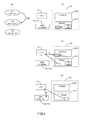
- FIG. 1 is a block diagram showing a structural example of a computer for implementing the present invention.
- FIG. 2 is a diagram showing the transition of the operation state of ACPI to which the present invention is applicable.
- FIG. 3 is an image diagram of the operation state in an example of the present invention.
- FIG. 4 is an image diagram of the operation state in an example of the present invention.
- FIG. 5 is an image diagram of the operation state in an example of the present invention.
- FIG. 6 is an image diagram of the operation state in an example of the present invention.
- FIG. 1 is a block diagram showing a structural example of a computer for implementing a method according to the present invention.
- a computer 100 includes a processor (hereafter referred to as “CPU”) 10 , storage means 20 , and various interfaces (hereafter referred to as “I/Fs”) 40 , which are connected to each other via a bus 30 .
- the various I/Fs 40 are a collective term for I/Fs including an input I/F, an output I/F, an external storage I/F, and an external communication I/F.
- Each I/F is connected to a corresponding one of input means 50 such as a keyboard and a mouse, display means 60 such as a CRT and an LCD, and external storage means 70 such as USB-connected semiconductor memory and an HDD.
- the storage means 20 can include an HDD, semiconductor memory such as RAM or ROM, and the like.
- the storage means 20 includes DRAM 210 and NVRAM 220 that function as main memory 200 .
- the NVRAM 220 can include any nonvolatile memory, such as EEPROM or flash memory, which is basically capable of storing data without continuous power supply.
- the method according to the present invention is implemented by the computer 100 executing predetermined software (including OS) stored in the storage means 20 or 70 or the like, as an example.
- FIG. 2 is a diagram showing the transition of the operation state of ACPI to which the present invention is applicable.
- ACPI stands for Advanced Configuration and Power Interface, which is an open unified standard for power control and configuration of PC/AT compatibles and the like.
- the application of the present invention is not limited to ACPI, and the present invention may be implemented based on any other standard or the like having the form (specification) equally involving the transition of the operation state of the computer.
- ACPI defines six states S 0 to S 5 as the operation state of the computer. Of these states, the present invention particularly focuses on the three states S 0 , S 4 , and S 5 .
- the three states S 0 , S 4 , and S 5 have the following meanings.
- the management of the main memory corresponding to the following three state transitions between the above-mentioned three states is executed as described later.
- the state transition T 50 is a state transition from power off (S 5 ) to normal operation (S 0 ) of the computer upon start (cold start), as shown in (a) in FIG. 3 .
- the condition of moving and storing data and the like between the elements is shown in (b) in FIG. 3 .
- a BIOS boot loader calls an OS boot loader.
- the OS boot loader loads programs and data from the HDD, etc. 20 ( 70 ) into the DRAM 210 , as indicated by arrow A.
- the OS boot loader also loads programs and data known to be read-only into the NVRAM 220 , as indicated by arrow B.
- an input/output buffer for a network device or an external storage is mapped onto the DRAM 210 because it is frequently written.
- the state transition T 04 is a state transition from normal operation (S 0 ) to hibernation (S 4 ) of the computer, as shown in (a) in FIG. 4 .
- the condition of moving and storing data and the like between the elements is shown in (b), (c), and (d) in FIG. 4 .
- data and the like and a page table are stored in the DRAM 210 .
- data in the DRAM 210 is moved to the NVRAM 220 on a page basis (hereafter “page” is also used with the same meaning as “data”) (arrow A).
- the page table is updated to store in the NVRAM 220 .
- the dotted arrow from the page table in each of (b) and (c) in FIG. 4 represents a pointer for specifying an area (address) in the memory. The same applies to FIGS. 5 and 6 described later.
- data is moved to the HDD, etc. 20 ( 70 ) (arrow B).
- the page table is moved to the NVRAM 220 last.
- the state transition T 40 is a state transition from hibernation (S 4 ) to normal operation (S 0 ) of the computer, as shown in (a) in FIG. 5 .
- the condition of moving and storing data and the like between the elements is shown in (b), (c), and (d) in FIG. 5 .
- the CPU 10 executes a program while reading data directly from the NVRAM 220 .
- the page table is moved to the DRAM 210 .
- each page mapped on the NVRAM 220 is assigned a read-only attribute.
- An option of moving a page in the DRAM 210 to the NVRAM 220 may be provided in order to reduce the amount of data moved in the state transition T 04 described with reference to FIG. 4 and to reduce the usage of the DRAM 210 to free up space. This is described below, with reference to FIG. 6 .
- the use state of the page table in the DRAM 210 is scanned (arrow Scan), as shown in (b) in FIG. 6 .
- a page in the DRAM 210 is moved to the NVRAM 220 (arrow Move), as shown in (c) in FIG. 6 .
- Whether to use condition 1 or condition 2 may be determined appropriately.
- the auxiliary operation can be called from a program, such as the kscand or kswapd routine, running periodically in Linux®.
- a program such as the kscand or kswapd routine, running periodically in Linux®.
- Other examples of the trigger to start the scan include: when the operating ratio of the CPU 10 is less than or equal to a predetermined value; and when no user input has been made for a predetermined time (e.g. screen saver start timing).
- the NVRAM is used as a part of the main memory (as a complement/reinforcement to the DRAM) or as a data backup destination depending on the operation state of the computer. This allows the computer to operate faster or with less power using the main memory.
- the method further includes: a step of detecting a use state of the DRAM; and a step of moving a page in the DRAM that has not been read for a time T 1 or has not been written for a time T 2 , to the NVRAM.
- data is moved to the NVRAM beforehand depending on the use state of the DRAM. This increases the free space in the DRAM, and reduces the amount of data moved when the computer operation is suspended.
- the step of detecting a use state of the DRAM is performed: (i) at predetermined time intervals; (ii) in the case where an operating ratio of a processor in the computer is less than or equal to a predetermined value; or (iii) in the case where no input to the computer has been made for a predetermined time.
- data is saved into the NVRAM beforehand depending on the operating condition of the computer (CPU). This increases the free space in the DRAM, and reduces the amount of data moved when the computer operation is suspended.
- the step (b) of moving data in the DRAM to the NVRAM on a page basis includes a step of moving data in the DRAM to an external storage device.
- the external storage device complements a lack of space of the NVRAM. As a result, data can be moved smoothly and securely when the computer operation is suspended.
- the present invention may be a system, a method, and/or a computer program product.
- the computer program product may include a computer readable storage medium (or media) having computer readable program instructions thereon for causing a processor to carry out aspects of the present invention.
- the computer readable storage medium can be a tangible device that can retain and store instructions for use by an instruction execution device.
- the computer readable storage medium may be, for example, but is not limited to, an electronic storage device, a magnetic storage device, an optical storage device, an electromagnetic storage device, a semiconductor storage device, or any suitable combination of the foregoing.
- a non-exhaustive list of more specific examples of the computer readable storage medium includes the following: a portable computer diskette, a hard disk, a random access memory (RAM), a read-only memory (ROM), an erasable programmable read-only memory (EPROM or Flash memory), a static random access memory (SRAM), a portable compact disc read-only memory (CD-ROM), a digital versatile disk (DVD), a memory stick, a floppy disk, a mechanically encoded device such as punch-cards or raised structures in a groove having instructions recorded thereon, and any suitable combination of the foregoing.
- RAM random access memory
- ROM read-only memory
- EPROM or Flash memory erasable programmable read-only memory
- SRAM static random access memory
- CD-ROM compact disc read-only memory
- DVD digital versatile disk
- memory stick a floppy disk
- a mechanically encoded device such as punch-cards or raised structures in a groove having instructions recorded thereon
- a computer readable storage medium is not to be construed as being transitory signals per se, such as radio waves or other freely propagating electromagnetic waves, electromagnetic waves propagating through a waveguide or other transmission media (e.g., light pulses passing through a fiber-optic cable), or electrical signals transmitted through a wire.
- Computer readable program instructions described herein can be downloaded to respective computing/processing devices from a computer readable storage medium or to an external computer or external storage device via a network, for example, the Internet, a local area network, a wide area network and/or a wireless network.
- the network may comprise copper transmission cables, optical transmission fibers, wireless transmission, routers, firewalls, switches, gateway computers and/or edge servers.
- a network adapter card or network interface in each computing/processing device receives computer readable program instructions from the network and forwards the computer readable program instructions for storage in a computer readable storage medium within the respective computing/processing device.
- Computer readable program instructions for carrying out operations of the present invention may be assembler instructions, instruction-set-architecture (ISA) instructions, machine instructions, machine dependent instructions, microcode, firmware instructions, state-setting data, or either source code or object code written in any combination of one or more programming languages, including an object oriented programming language such as Smalltalk, C++ or the like, and conventional procedural programming languages, such as the “C” programming language or similar programming languages.
- the computer readable program instructions may execute entirely on the user's computer, partly on the user's computer, as a stand-alone software package, partly on the user's computer and partly on a remote computer or entirely on the remote computer or server.
- the remote computer may be connected to the user's computer through any type of network, including a local area network (LAN) or a wide area network (WAN), or the connection may be made to an external computer (for example, through the Internet using an Internet Service Provider).
- electronic circuitry including, for example, programmable logic circuitry, field-programmable gate arrays (FPGA), or programmable logic arrays (PLA) may execute the computer readable program instructions by utilizing state information of the computer readable program instructions to personalize the electronic circuitry, in order to perform aspects of the present invention.
- These computer readable program instructions may be provided to a processor of a general purpose computer, special purpose computer, or other programmable data processing apparatus to produce a machine, such that the instructions, which execute via the processor of the computer or other programmable data processing apparatus, create means for implementing the functions/acts specified in the flowchart and/or block diagram block or blocks.
- These computer readable program instructions may also be stored in a computer readable storage medium that can direct a computer, a programmable data processing apparatus, and/or other devices to function in a particular manner, such that the computer readable storage medium having instructions stored therein comprises an article of manufacture including instructions which implement aspects of the function/act specified in the flowchart and/or block diagram block or blocks.
- the computer readable program instructions may also be loaded onto a computer, other programmable data processing apparatus, or other device to cause a series of operational steps to be performed on the computer, other programmable apparatus or other device to produce a computer implemented process, such that the instructions which execute on the computer, other programmable apparatus, or other device implement the functions/acts specified in the flowchart and/or block diagram block or blocks.
- each block in the flowchart or block diagrams may represent a module, segment, or portion of instructions, which comprises one or more executable instructions for implementing the specified logical function(s).
- the functions noted in the block may occur out of the order noted in the figures.
- two blocks shown in succession may, in fact, be executed substantially concurrently, or the blocks may sometimes be executed in the reverse order, depending upon the functionality involved.
Abstract
Description
-
- S0: normal operation state
- S4: a state called suspend to disk or hibernation where the contents of memory are lost, which is the same as writing the contents of memory to an HDD or the like and powering off
- S5: complete power off
-
- T50: S5→S0
- T04: S0→S4
- T40: S4→S0
-
- Condition 1: move a page in the
DRAM 210 that has not been used for the past Tu seconds, to theNVRAM 220 - Condition 2: move a page in the
DRAM 210 that has not been written for the past Tw seconds, to theNVRAM 220
- Condition 1: move a page in the
Claims (12)
Priority Applications (1)
| Application Number | Priority Date | Filing Date | Title |
|---|---|---|---|
| US15/349,391 US9891854B2 (en) | 2014-06-17 | 2016-11-11 | Memory management method |
Applications Claiming Priority (2)
| Application Number | Priority Date | Filing Date | Title |
|---|---|---|---|
| JP2014124370A JP5901698B2 (en) | 2014-06-17 | 2014-06-17 | Memory management method |
| JP2014-124370 | 2014-06-17 |
Related Child Applications (1)
| Application Number | Title | Priority Date | Filing Date |
|---|---|---|---|
| US15/349,391 Continuation US9891854B2 (en) | 2014-06-17 | 2016-11-11 | Memory management method |
Publications (2)
| Publication Number | Publication Date |
|---|---|
| US20150363311A1 US20150363311A1 (en) | 2015-12-17 |
| US9552291B2 true US9552291B2 (en) | 2017-01-24 |
Family
ID=54836261
Family Applications (2)
| Application Number | Title | Priority Date | Filing Date |
|---|---|---|---|
| US14/722,532 Expired - Fee Related US9552291B2 (en) | 2014-06-17 | 2015-05-27 | Memory management method |
| US15/349,391 Expired - Fee Related US9891854B2 (en) | 2014-06-17 | 2016-11-11 | Memory management method |
Family Applications After (1)
| Application Number | Title | Priority Date | Filing Date |
|---|---|---|---|
| US15/349,391 Expired - Fee Related US9891854B2 (en) | 2014-06-17 | 2016-11-11 | Memory management method |
Country Status (2)
| Country | Link |
|---|---|
| US (2) | US9552291B2 (en) |
| JP (1) | JP5901698B2 (en) |
Cited By (76)
| Publication number | Priority date | Publication date | Assignee | Title |
|---|---|---|---|---|
| US10817431B2 (en) | 2014-07-02 | 2020-10-27 | Pure Storage, Inc. | Distributed storage addressing |
| US10838633B2 (en) | 2014-06-04 | 2020-11-17 | Pure Storage, Inc. | Configurable hyperconverged multi-tenant storage system |
| US10942869B2 (en) | 2017-03-30 | 2021-03-09 | Pure Storage, Inc. | Efficient coding in a storage system |
| US11030090B2 (en) | 2016-07-26 | 2021-06-08 | Pure Storage, Inc. | Adaptive data migration |
| US11074016B2 (en) | 2017-10-31 | 2021-07-27 | Pure Storage, Inc. | Using flash storage devices with different sized erase blocks |
| US11079962B2 (en) | 2014-07-02 | 2021-08-03 | Pure Storage, Inc. | Addressable non-volatile random access memory |
| US11086532B2 (en) | 2017-10-31 | 2021-08-10 | Pure Storage, Inc. | Data rebuild with changing erase block sizes |
| US11099986B2 (en) | 2019-04-12 | 2021-08-24 | Pure Storage, Inc. | Efficient transfer of memory contents |
| US11138082B2 (en) | 2014-06-04 | 2021-10-05 | Pure Storage, Inc. | Action determination based on redundancy level |
| US11144212B2 (en) | 2015-04-10 | 2021-10-12 | Pure Storage, Inc. | Independent partitions within an array |
| US11188476B1 (en) | 2014-08-20 | 2021-11-30 | Pure Storage, Inc. | Virtual addressing in a storage system |
| US11190580B2 (en) | 2017-07-03 | 2021-11-30 | Pure Storage, Inc. | Stateful connection resets |
| US11204701B2 (en) | 2015-12-22 | 2021-12-21 | Pure Storage, Inc. | Token based transactions |
| US11204830B2 (en) | 2014-08-07 | 2021-12-21 | Pure Storage, Inc. | Die-level monitoring in a storage cluster |
| US11240307B2 (en) | 2015-04-09 | 2022-02-01 | Pure Storage, Inc. | Multiple communication paths in a storage system |
| US11289169B2 (en) | 2017-01-13 | 2022-03-29 | Pure Storage, Inc. | Cycled background reads |
| US11307998B2 (en) | 2017-01-09 | 2022-04-19 | Pure Storage, Inc. | Storage efficiency of encrypted host system data |
| US11310317B1 (en) | 2014-06-04 | 2022-04-19 | Pure Storage, Inc. | Efficient load balancing |
| US11340821B2 (en) | 2016-07-26 | 2022-05-24 | Pure Storage, Inc. | Adjustable migration utilization |
| US11354058B2 (en) | 2018-09-06 | 2022-06-07 | Pure Storage, Inc. | Local relocation of data stored at a storage device of a storage system |
| US11385799B2 (en) | 2014-06-04 | 2022-07-12 | Pure Storage, Inc. | Storage nodes supporting multiple erasure coding schemes |
| US11385979B2 (en) | 2014-07-02 | 2022-07-12 | Pure Storage, Inc. | Mirrored remote procedure call cache |
| US11392522B2 (en) | 2014-07-03 | 2022-07-19 | Pure Storage, Inc. | Transfer of segmented data |
| US11409437B2 (en) | 2016-07-22 | 2022-08-09 | Pure Storage, Inc. | Persisting configuration information |
| US11416144B2 (en) | 2019-12-12 | 2022-08-16 | Pure Storage, Inc. | Dynamic use of segment or zone power loss protection in a flash device |
| US11442645B2 (en) | 2018-01-31 | 2022-09-13 | Pure Storage, Inc. | Distributed storage system expansion mechanism |
| US11442625B2 (en) | 2014-08-07 | 2022-09-13 | Pure Storage, Inc. | Multiple read data paths in a storage system |
| US11489668B2 (en) | 2015-09-30 | 2022-11-01 | Pure Storage, Inc. | Secret regeneration in a storage system |
| US11494498B2 (en) | 2014-07-03 | 2022-11-08 | Pure Storage, Inc. | Storage data decryption |
| US11507597B2 (en) | 2021-03-31 | 2022-11-22 | Pure Storage, Inc. | Data replication to meet a recovery point objective |
| US11544143B2 (en) | 2014-08-07 | 2023-01-03 | Pure Storage, Inc. | Increased data reliability |
| US11550473B2 (en) | 2016-05-03 | 2023-01-10 | Pure Storage, Inc. | High-availability storage array |
| US11550752B2 (en) | 2014-07-03 | 2023-01-10 | Pure Storage, Inc. | Administrative actions via a reserved filename |
| US11567917B2 (en) | 2015-09-30 | 2023-01-31 | Pure Storage, Inc. | Writing data and metadata into storage |
| US11582046B2 (en) | 2015-10-23 | 2023-02-14 | Pure Storage, Inc. | Storage system communication |
| US11592985B2 (en) | 2017-04-05 | 2023-02-28 | Pure Storage, Inc. | Mapping LUNs in a storage memory |
| US11593203B2 (en) | 2014-06-04 | 2023-02-28 | Pure Storage, Inc. | Coexisting differing erasure codes |
| US11604690B2 (en) | 2016-07-24 | 2023-03-14 | Pure Storage, Inc. | Online failure span determination |
| US11604598B2 (en) | 2014-07-02 | 2023-03-14 | Pure Storage, Inc. | Storage cluster with zoned drives |
| US11614880B2 (en) | 2020-12-31 | 2023-03-28 | Pure Storage, Inc. | Storage system with selectable write paths |
| US11620197B2 (en) | 2014-08-07 | 2023-04-04 | Pure Storage, Inc. | Recovering error corrected data |
| US11650976B2 (en) | 2011-10-14 | 2023-05-16 | Pure Storage, Inc. | Pattern matching using hash tables in storage system |
| US11652884B2 (en) | 2014-06-04 | 2023-05-16 | Pure Storage, Inc. | Customized hash algorithms |
| US11656961B2 (en) | 2020-02-28 | 2023-05-23 | Pure Storage, Inc. | Deallocation within a storage system |
| US11656768B2 (en) | 2016-09-15 | 2023-05-23 | Pure Storage, Inc. | File deletion in a distributed system |
| US11675762B2 (en) | 2015-06-26 | 2023-06-13 | Pure Storage, Inc. | Data structures for key management |
| US11704192B2 (en) | 2019-12-12 | 2023-07-18 | Pure Storage, Inc. | Budgeting open blocks based on power loss protection |
| US11704073B2 (en) | 2015-07-13 | 2023-07-18 | Pure Storage, Inc | Ownership determination for accessing a file |
| US11714708B2 (en) | 2017-07-31 | 2023-08-01 | Pure Storage, Inc. | Intra-device redundancy scheme |
| US11722455B2 (en) | 2017-04-27 | 2023-08-08 | Pure Storage, Inc. | Storage cluster address resolution |
| US11734169B2 (en) | 2016-07-26 | 2023-08-22 | Pure Storage, Inc. | Optimizing spool and memory space management |
| US11740802B2 (en) | 2015-09-01 | 2023-08-29 | Pure Storage, Inc. | Error correction bypass for erased pages |
| US11741003B2 (en) | 2017-11-17 | 2023-08-29 | Pure Storage, Inc. | Write granularity for storage system |
| US11775491B2 (en) | 2020-04-24 | 2023-10-03 | Pure Storage, Inc. | Machine learning model for storage system |
| US11775428B2 (en) | 2015-03-26 | 2023-10-03 | Pure Storage, Inc. | Deletion immunity for unreferenced data |
| US11782625B2 (en) | 2017-06-11 | 2023-10-10 | Pure Storage, Inc. | Heterogeneity supportive resiliency groups |
| US11789626B2 (en) | 2020-12-17 | 2023-10-17 | Pure Storage, Inc. | Optimizing block allocation in a data storage system |
| US11797212B2 (en) | 2016-07-26 | 2023-10-24 | Pure Storage, Inc. | Data migration for zoned drives |
| US11822444B2 (en) | 2014-06-04 | 2023-11-21 | Pure Storage, Inc. | Data rebuild independent of error detection |
| US11822807B2 (en) | 2019-06-24 | 2023-11-21 | Pure Storage, Inc. | Data replication in a storage system |
| US11836348B2 (en) | 2018-04-27 | 2023-12-05 | Pure Storage, Inc. | Upgrade for system with differing capacities |
| US11842053B2 (en) | 2016-12-19 | 2023-12-12 | Pure Storage, Inc. | Zone namespace |
| US11846968B2 (en) | 2018-09-06 | 2023-12-19 | Pure Storage, Inc. | Relocation of data for heterogeneous storage systems |
| US11847331B2 (en) | 2019-12-12 | 2023-12-19 | Pure Storage, Inc. | Budgeting open blocks of a storage unit based on power loss prevention |
| US11847013B2 (en) | 2018-02-18 | 2023-12-19 | Pure Storage, Inc. | Readable data determination |
| US11847324B2 (en) | 2020-12-31 | 2023-12-19 | Pure Storage, Inc. | Optimizing resiliency groups for data regions of a storage system |
| US11861188B2 (en) | 2016-07-19 | 2024-01-02 | Pure Storage, Inc. | System having modular accelerators |
| US11869583B2 (en) | 2017-04-27 | 2024-01-09 | Pure Storage, Inc. | Page write requirements for differing types of flash memory |
| US11868309B2 (en) | 2018-09-06 | 2024-01-09 | Pure Storage, Inc. | Queue management for data relocation |
| US11886308B2 (en) | 2014-07-02 | 2024-01-30 | Pure Storage, Inc. | Dual class of service for unified file and object messaging |
| US11886334B2 (en) | 2016-07-26 | 2024-01-30 | Pure Storage, Inc. | Optimizing spool and memory space management |
| US11886288B2 (en) | 2016-07-22 | 2024-01-30 | Pure Storage, Inc. | Optimize data protection layouts based on distributed flash wear leveling |
| US11893023B2 (en) | 2015-09-04 | 2024-02-06 | Pure Storage, Inc. | Deterministic searching using compressed indexes |
| US11893126B2 (en) | 2019-10-14 | 2024-02-06 | Pure Storage, Inc. | Data deletion for a multi-tenant environment |
| US11922070B2 (en) | 2016-10-04 | 2024-03-05 | Pure Storage, Inc. | Granting access to a storage device based on reservations |
| US11955187B2 (en) | 2022-02-28 | 2024-04-09 | Pure Storage, Inc. | Refresh of differing capacity NAND |
Families Citing this family (6)
| Publication number | Priority date | Publication date | Assignee | Title |
|---|---|---|---|---|
| CN105320621A (en) * | 2014-08-04 | 2016-02-10 | 株式会社东芝 | Memory system and information processing device |
| US9928168B2 (en) * | 2016-01-11 | 2018-03-27 | Qualcomm Incorporated | Non-volatile random access system memory with DRAM program caching |
| US9847105B2 (en) * | 2016-02-01 | 2017-12-19 | Samsung Electric Co., Ltd. | Memory package, memory module including the same, and operation method of memory package |
| WO2017145360A1 (en) * | 2016-02-26 | 2017-08-31 | 三菱電機株式会社 | Information processing device and information processing method |
| US10942844B2 (en) * | 2016-06-10 | 2021-03-09 | Apple Inc. | Reserved memory in memory management system |
| CN108572799B (en) * | 2018-04-12 | 2021-05-04 | 上海理工大学 | Data page migration method of heterogeneous memory system of bidirectional hash chain table |
Citations (11)
| Publication number | Priority date | Publication date | Assignee | Title |
|---|---|---|---|---|
| JP2004362426A (en) | 2003-06-06 | 2004-12-24 | Sony Corp | Information processing system, its control method, and computer program |
| JP2005010897A (en) | 2003-06-17 | 2005-01-13 | Nec Corp | Computer system, computer system starting method and program |
| WO2006028658A1 (en) | 2004-09-03 | 2006-03-16 | Intel Corporation | Storing system information in a low-latency persistent memory device upon transition to a lower-power state |
| US20080109592A1 (en) * | 2006-11-04 | 2008-05-08 | Virident Systems Inc. | Seamless application access to hybrid main memory |
| JP2009093502A (en) | 2007-10-10 | 2009-04-30 | Canon Inc | Information processing apparatus and control method thereof |
| US20090172439A1 (en) * | 2007-12-28 | 2009-07-02 | Intel Corporation | System and method for fast platform hibernate and resume |
| JP2010282252A (en) | 2009-06-02 | 2010-12-16 | Ubiquitous Corp | Program, control method, and controller |
| US20130077382A1 (en) * | 2011-09-26 | 2013-03-28 | Samsung Electronics Co., Ltd. | Hybrid memory device, system including the same, and method of reading and writing data in the hybrid memory device |
| US20130283079A1 (en) * | 2011-12-13 | 2013-10-24 | Leena K. Puthiyedath | Method and system for providing instant responses to sleep state transitions with non-volatile random access memory |
| US20130290759A1 (en) * | 2011-12-13 | 2013-10-31 | Mohan J. Kumar | Enhanced system sleep state support in servers using non-volatile random access memory |
| JP2014232525A (en) | 2013-04-30 | 2014-12-11 | 株式会社半導体エネルギー研究所 | Semiconductor device |
-
2014
- 2014-06-17 JP JP2014124370A patent/JP5901698B2/en not_active Expired - Fee Related
-
2015
- 2015-05-27 US US14/722,532 patent/US9552291B2/en not_active Expired - Fee Related
-
2016
- 2016-11-11 US US15/349,391 patent/US9891854B2/en not_active Expired - Fee Related
Patent Citations (11)
| Publication number | Priority date | Publication date | Assignee | Title |
|---|---|---|---|---|
| JP2004362426A (en) | 2003-06-06 | 2004-12-24 | Sony Corp | Information processing system, its control method, and computer program |
| JP2005010897A (en) | 2003-06-17 | 2005-01-13 | Nec Corp | Computer system, computer system starting method and program |
| WO2006028658A1 (en) | 2004-09-03 | 2006-03-16 | Intel Corporation | Storing system information in a low-latency persistent memory device upon transition to a lower-power state |
| US20080109592A1 (en) * | 2006-11-04 | 2008-05-08 | Virident Systems Inc. | Seamless application access to hybrid main memory |
| JP2009093502A (en) | 2007-10-10 | 2009-04-30 | Canon Inc | Information processing apparatus and control method thereof |
| US20090172439A1 (en) * | 2007-12-28 | 2009-07-02 | Intel Corporation | System and method for fast platform hibernate and resume |
| JP2010282252A (en) | 2009-06-02 | 2010-12-16 | Ubiquitous Corp | Program, control method, and controller |
| US20130077382A1 (en) * | 2011-09-26 | 2013-03-28 | Samsung Electronics Co., Ltd. | Hybrid memory device, system including the same, and method of reading and writing data in the hybrid memory device |
| US20130283079A1 (en) * | 2011-12-13 | 2013-10-24 | Leena K. Puthiyedath | Method and system for providing instant responses to sleep state transitions with non-volatile random access memory |
| US20130290759A1 (en) * | 2011-12-13 | 2013-10-31 | Mohan J. Kumar | Enhanced system sleep state support in servers using non-volatile random access memory |
| JP2014232525A (en) | 2013-04-30 | 2014-12-11 | 株式会社半導体エネルギー研究所 | Semiconductor device |
Non-Patent Citations (4)
| Title |
|---|
| Mogul et al., "Operating System Support for NVM+DRAM Hybrid Main Memory", HP Labs, Palo Alto, CA and Barcelona, Spain, pp. 1-5. |
| Translation of Japan Application No. 2014-124370, filed Jun. 17, 2014, entitled: "Memory Management Method", (20 pages). |
| Wu et al., "eNVy: A Non-Volatile, Main Memory Storage System", 1993 IEEE, pp. 116-118. |
| Yoon et al., "Row Buffer Locality Aware Caching Policies for Hybrid Memories", Carnegie Mellon University, (pp. 1-8). |
Cited By (93)
| Publication number | Priority date | Publication date | Assignee | Title |
|---|---|---|---|---|
| US11650976B2 (en) | 2011-10-14 | 2023-05-16 | Pure Storage, Inc. | Pattern matching using hash tables in storage system |
| US11500552B2 (en) | 2014-06-04 | 2022-11-15 | Pure Storage, Inc. | Configurable hyperconverged multi-tenant storage system |
| US11310317B1 (en) | 2014-06-04 | 2022-04-19 | Pure Storage, Inc. | Efficient load balancing |
| US11671496B2 (en) | 2014-06-04 | 2023-06-06 | Pure Storage, Inc. | Load balacing for distibuted computing |
| US11138082B2 (en) | 2014-06-04 | 2021-10-05 | Pure Storage, Inc. | Action determination based on redundancy level |
| US11385799B2 (en) | 2014-06-04 | 2022-07-12 | Pure Storage, Inc. | Storage nodes supporting multiple erasure coding schemes |
| US11593203B2 (en) | 2014-06-04 | 2023-02-28 | Pure Storage, Inc. | Coexisting differing erasure codes |
| US11652884B2 (en) | 2014-06-04 | 2023-05-16 | Pure Storage, Inc. | Customized hash algorithms |
| US10838633B2 (en) | 2014-06-04 | 2020-11-17 | Pure Storage, Inc. | Configurable hyperconverged multi-tenant storage system |
| US11822444B2 (en) | 2014-06-04 | 2023-11-21 | Pure Storage, Inc. | Data rebuild independent of error detection |
| US11604598B2 (en) | 2014-07-02 | 2023-03-14 | Pure Storage, Inc. | Storage cluster with zoned drives |
| US11886308B2 (en) | 2014-07-02 | 2024-01-30 | Pure Storage, Inc. | Dual class of service for unified file and object messaging |
| US11385979B2 (en) | 2014-07-02 | 2022-07-12 | Pure Storage, Inc. | Mirrored remote procedure call cache |
| US10817431B2 (en) | 2014-07-02 | 2020-10-27 | Pure Storage, Inc. | Distributed storage addressing |
| US11922046B2 (en) | 2014-07-02 | 2024-03-05 | Pure Storage, Inc. | Erasure coded data within zoned drives |
| US11079962B2 (en) | 2014-07-02 | 2021-08-03 | Pure Storage, Inc. | Addressable non-volatile random access memory |
| US11392522B2 (en) | 2014-07-03 | 2022-07-19 | Pure Storage, Inc. | Transfer of segmented data |
| US11928076B2 (en) | 2014-07-03 | 2024-03-12 | Pure Storage, Inc. | Actions for reserved filenames |
| US11550752B2 (en) | 2014-07-03 | 2023-01-10 | Pure Storage, Inc. | Administrative actions via a reserved filename |
| US11494498B2 (en) | 2014-07-03 | 2022-11-08 | Pure Storage, Inc. | Storage data decryption |
| US11620197B2 (en) | 2014-08-07 | 2023-04-04 | Pure Storage, Inc. | Recovering error corrected data |
| US11656939B2 (en) | 2014-08-07 | 2023-05-23 | Pure Storage, Inc. | Storage cluster memory characterization |
| US11544143B2 (en) | 2014-08-07 | 2023-01-03 | Pure Storage, Inc. | Increased data reliability |
| US11204830B2 (en) | 2014-08-07 | 2021-12-21 | Pure Storage, Inc. | Die-level monitoring in a storage cluster |
| US11442625B2 (en) | 2014-08-07 | 2022-09-13 | Pure Storage, Inc. | Multiple read data paths in a storage system |
| US11734186B2 (en) | 2014-08-20 | 2023-08-22 | Pure Storage, Inc. | Heterogeneous storage with preserved addressing |
| US11188476B1 (en) | 2014-08-20 | 2021-11-30 | Pure Storage, Inc. | Virtual addressing in a storage system |
| US11775428B2 (en) | 2015-03-26 | 2023-10-03 | Pure Storage, Inc. | Deletion immunity for unreferenced data |
| US11722567B2 (en) | 2015-04-09 | 2023-08-08 | Pure Storage, Inc. | Communication paths for storage devices having differing capacities |
| US11240307B2 (en) | 2015-04-09 | 2022-02-01 | Pure Storage, Inc. | Multiple communication paths in a storage system |
| US11144212B2 (en) | 2015-04-10 | 2021-10-12 | Pure Storage, Inc. | Independent partitions within an array |
| US11675762B2 (en) | 2015-06-26 | 2023-06-13 | Pure Storage, Inc. | Data structures for key management |
| US11704073B2 (en) | 2015-07-13 | 2023-07-18 | Pure Storage, Inc | Ownership determination for accessing a file |
| US11740802B2 (en) | 2015-09-01 | 2023-08-29 | Pure Storage, Inc. | Error correction bypass for erased pages |
| US11893023B2 (en) | 2015-09-04 | 2024-02-06 | Pure Storage, Inc. | Deterministic searching using compressed indexes |
| US11838412B2 (en) | 2015-09-30 | 2023-12-05 | Pure Storage, Inc. | Secret regeneration from distributed shares |
| US11489668B2 (en) | 2015-09-30 | 2022-11-01 | Pure Storage, Inc. | Secret regeneration in a storage system |
| US11567917B2 (en) | 2015-09-30 | 2023-01-31 | Pure Storage, Inc. | Writing data and metadata into storage |
| US11582046B2 (en) | 2015-10-23 | 2023-02-14 | Pure Storage, Inc. | Storage system communication |
| US11204701B2 (en) | 2015-12-22 | 2021-12-21 | Pure Storage, Inc. | Token based transactions |
| US11550473B2 (en) | 2016-05-03 | 2023-01-10 | Pure Storage, Inc. | High-availability storage array |
| US11847320B2 (en) | 2016-05-03 | 2023-12-19 | Pure Storage, Inc. | Reassignment of requests for high availability |
| US11861188B2 (en) | 2016-07-19 | 2024-01-02 | Pure Storage, Inc. | System having modular accelerators |
| US11409437B2 (en) | 2016-07-22 | 2022-08-09 | Pure Storage, Inc. | Persisting configuration information |
| US11886288B2 (en) | 2016-07-22 | 2024-01-30 | Pure Storage, Inc. | Optimize data protection layouts based on distributed flash wear leveling |
| US11604690B2 (en) | 2016-07-24 | 2023-03-14 | Pure Storage, Inc. | Online failure span determination |
| US11797212B2 (en) | 2016-07-26 | 2023-10-24 | Pure Storage, Inc. | Data migration for zoned drives |
| US11886334B2 (en) | 2016-07-26 | 2024-01-30 | Pure Storage, Inc. | Optimizing spool and memory space management |
| US11030090B2 (en) | 2016-07-26 | 2021-06-08 | Pure Storage, Inc. | Adaptive data migration |
| US11340821B2 (en) | 2016-07-26 | 2022-05-24 | Pure Storage, Inc. | Adjustable migration utilization |
| US11734169B2 (en) | 2016-07-26 | 2023-08-22 | Pure Storage, Inc. | Optimizing spool and memory space management |
| US11656768B2 (en) | 2016-09-15 | 2023-05-23 | Pure Storage, Inc. | File deletion in a distributed system |
| US11922033B2 (en) | 2016-09-15 | 2024-03-05 | Pure Storage, Inc. | Batch data deletion |
| US11922070B2 (en) | 2016-10-04 | 2024-03-05 | Pure Storage, Inc. | Granting access to a storage device based on reservations |
| US11842053B2 (en) | 2016-12-19 | 2023-12-12 | Pure Storage, Inc. | Zone namespace |
| US11307998B2 (en) | 2017-01-09 | 2022-04-19 | Pure Storage, Inc. | Storage efficiency of encrypted host system data |
| US11289169B2 (en) | 2017-01-13 | 2022-03-29 | Pure Storage, Inc. | Cycled background reads |
| US10942869B2 (en) | 2017-03-30 | 2021-03-09 | Pure Storage, Inc. | Efficient coding in a storage system |
| US11592985B2 (en) | 2017-04-05 | 2023-02-28 | Pure Storage, Inc. | Mapping LUNs in a storage memory |
| US11869583B2 (en) | 2017-04-27 | 2024-01-09 | Pure Storage, Inc. | Page write requirements for differing types of flash memory |
| US11722455B2 (en) | 2017-04-27 | 2023-08-08 | Pure Storage, Inc. | Storage cluster address resolution |
| US11782625B2 (en) | 2017-06-11 | 2023-10-10 | Pure Storage, Inc. | Heterogeneity supportive resiliency groups |
| US11190580B2 (en) | 2017-07-03 | 2021-11-30 | Pure Storage, Inc. | Stateful connection resets |
| US11689610B2 (en) | 2017-07-03 | 2023-06-27 | Pure Storage, Inc. | Load balancing reset packets |
| US11714708B2 (en) | 2017-07-31 | 2023-08-01 | Pure Storage, Inc. | Intra-device redundancy scheme |
| US11086532B2 (en) | 2017-10-31 | 2021-08-10 | Pure Storage, Inc. | Data rebuild with changing erase block sizes |
| US11604585B2 (en) | 2017-10-31 | 2023-03-14 | Pure Storage, Inc. | Data rebuild when changing erase block sizes during drive replacement |
| US11074016B2 (en) | 2017-10-31 | 2021-07-27 | Pure Storage, Inc. | Using flash storage devices with different sized erase blocks |
| US11704066B2 (en) | 2017-10-31 | 2023-07-18 | Pure Storage, Inc. | Heterogeneous erase blocks |
| US11741003B2 (en) | 2017-11-17 | 2023-08-29 | Pure Storage, Inc. | Write granularity for storage system |
| US11797211B2 (en) | 2018-01-31 | 2023-10-24 | Pure Storage, Inc. | Expanding data structures in a storage system |
| US11442645B2 (en) | 2018-01-31 | 2022-09-13 | Pure Storage, Inc. | Distributed storage system expansion mechanism |
| US11847013B2 (en) | 2018-02-18 | 2023-12-19 | Pure Storage, Inc. | Readable data determination |
| US11836348B2 (en) | 2018-04-27 | 2023-12-05 | Pure Storage, Inc. | Upgrade for system with differing capacities |
| US11354058B2 (en) | 2018-09-06 | 2022-06-07 | Pure Storage, Inc. | Local relocation of data stored at a storage device of a storage system |
| US11846968B2 (en) | 2018-09-06 | 2023-12-19 | Pure Storage, Inc. | Relocation of data for heterogeneous storage systems |
| US11868309B2 (en) | 2018-09-06 | 2024-01-09 | Pure Storage, Inc. | Queue management for data relocation |
| US11099986B2 (en) | 2019-04-12 | 2021-08-24 | Pure Storage, Inc. | Efficient transfer of memory contents |
| US11899582B2 (en) | 2019-04-12 | 2024-02-13 | Pure Storage, Inc. | Efficient memory dump |
| US11822807B2 (en) | 2019-06-24 | 2023-11-21 | Pure Storage, Inc. | Data replication in a storage system |
| US11893126B2 (en) | 2019-10-14 | 2024-02-06 | Pure Storage, Inc. | Data deletion for a multi-tenant environment |
| US11847331B2 (en) | 2019-12-12 | 2023-12-19 | Pure Storage, Inc. | Budgeting open blocks of a storage unit based on power loss prevention |
| US11947795B2 (en) | 2019-12-12 | 2024-04-02 | Pure Storage, Inc. | Power loss protection based on write requirements |
| US11704192B2 (en) | 2019-12-12 | 2023-07-18 | Pure Storage, Inc. | Budgeting open blocks based on power loss protection |
| US11416144B2 (en) | 2019-12-12 | 2022-08-16 | Pure Storage, Inc. | Dynamic use of segment or zone power loss protection in a flash device |
| US11656961B2 (en) | 2020-02-28 | 2023-05-23 | Pure Storage, Inc. | Deallocation within a storage system |
| US11775491B2 (en) | 2020-04-24 | 2023-10-03 | Pure Storage, Inc. | Machine learning model for storage system |
| US11789626B2 (en) | 2020-12-17 | 2023-10-17 | Pure Storage, Inc. | Optimizing block allocation in a data storage system |
| US11614880B2 (en) | 2020-12-31 | 2023-03-28 | Pure Storage, Inc. | Storage system with selectable write paths |
| US11847324B2 (en) | 2020-12-31 | 2023-12-19 | Pure Storage, Inc. | Optimizing resiliency groups for data regions of a storage system |
| US11507597B2 (en) | 2021-03-31 | 2022-11-22 | Pure Storage, Inc. | Data replication to meet a recovery point objective |
| US11960371B2 (en) | 2021-09-30 | 2024-04-16 | Pure Storage, Inc. | Message persistence in a zoned system |
| US11955187B2 (en) | 2022-02-28 | 2024-04-09 | Pure Storage, Inc. | Refresh of differing capacity NAND |
Also Published As
| Publication number | Publication date |
|---|---|
| JP5901698B2 (en) | 2016-04-13 |
| JP2016004420A (en) | 2016-01-12 |
| US9891854B2 (en) | 2018-02-13 |
| US20150363311A1 (en) | 2015-12-17 |
| US20170075618A1 (en) | 2017-03-16 |
Similar Documents
| Publication | Publication Date | Title |
|---|---|---|
| US9891854B2 (en) | Memory management method | |
| US10705935B2 (en) | Generating job alert | |
| US10198189B2 (en) | Data allocation among devices with different data rates | |
| US10241813B2 (en) | Method and apparatus for patching | |
| US9665394B2 (en) | Sharing application objects among multiple tenants | |
| US11126454B2 (en) | Enforcing retention policies with respect to virtual machine snapshots | |
| US20140006768A1 (en) | Selectively allowing changes to a system | |
| US10209757B2 (en) | Reducing power consumption in a multi-slice computer processor | |
| US10069848B2 (en) | Method and system for data security | |
| US20130145382A1 (en) | Computing device and function module management method | |
| US10761755B2 (en) | Method and apparatus for reclaiming memory blocks in snapshot storage space | |
| US10297004B2 (en) | Multiple frame buffers for windowless embedded environment | |
| US10204045B2 (en) | Data file handling in a volatile memory | |
| US9104558B2 (en) | Preventing out-of-space errors for legacy option ROM in a computing system | |
| US11023348B2 (en) | Multi-layer autoscaling for a scale-up cloud server | |
| US9857979B2 (en) | Optimizing page boundary crossing in system memory using a reference bit and a change bit | |
| US9519583B1 (en) | Dedicated memory structure holding data for detecting available worker thread(s) and informing available worker thread(s) of task(s) to execute | |
| US10296337B2 (en) | Preventing premature reads from a general purpose register | |
| US20140181385A1 (en) | Flexible utilization of block storage in a computing system | |
| US9207927B2 (en) | Dynamic image composition method employing fenced applications |
Legal Events
| Date | Code | Title | Description |
|---|---|---|---|
| AS | Assignment |
Owner name: INTERNATIONAL BUSINESS MACHINES CORPORATION, NEW Y Free format text: ASSIGNMENT OF ASSIGNORS INTEREST;ASSIGNORS:MUNETOH, SEIJI;OHBA, NOBUYUKI;SIGNING DATES FROM 20150518 TO 20150519;REEL/FRAME:035721/0312 |
|
| STCF | Information on status: patent grant |
Free format text: PATENTED CASE |
|
| FEPP | Fee payment procedure |
Free format text: MAINTENANCE FEE REMINDER MAILED (ORIGINAL EVENT CODE: REM.); ENTITY STATUS OF PATENT OWNER: LARGE ENTITY |
|
| LAPS | Lapse for failure to pay maintenance fees |
Free format text: PATENT EXPIRED FOR FAILURE TO PAY MAINTENANCE FEES (ORIGINAL EVENT CODE: EXP.); ENTITY STATUS OF PATENT OWNER: LARGE ENTITY |
|
| STCH | Information on status: patent discontinuation |
Free format text: PATENT EXPIRED DUE TO NONPAYMENT OF MAINTENANCE FEES UNDER 37 CFR 1.362 |
|
| FP | Lapsed due to failure to pay maintenance fee |
Effective date: 20210124 |